Loading...
News Article

EVG partners with Plessey on microLEDs

News
Companies to drive GaN-on-Silicon monolithic microLED technology for AR applications

Plessey has announced a collaboration with EV Group (EVG), a supplier of wafer bonding and lithography equipment to bring high-performance GaN-on-Silicon (GaN-on-Si) monolithic microLED technology to the mass market.

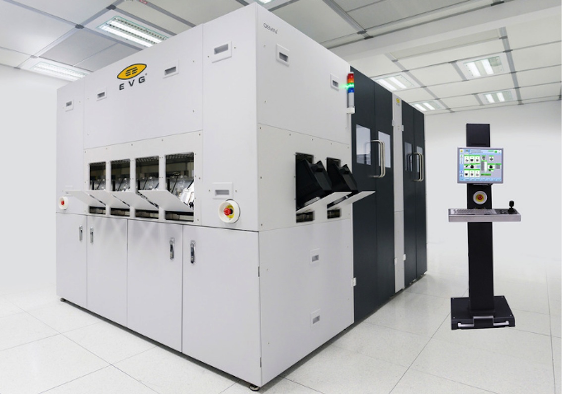
Plessey has purchased a GEMINI production wafer bonding system from EVG to enable bonding and alignment at Plessey’s fabrication facility in Plymouth, UK. This enables Plessey to bond its GaN-on-Si microLED arrays to the panel’s backplane at a wafer level, and with the high level of alignment precision necessary to enable very small pixel dimensions.

EVG’s patented SmartViewNT Automated Bond Alignment System technology is suitable for Plessey’s requirements because it allows face-to-face alignment of the wafers with very high precision. A maximum level of automation and process integration is achieved by the GEMINI Automated Production Wafer Bonding System. Wafer-to-wafer alignment and wafer bonding processes up to 300mm for volume manufacturing are all performed in one fully automated platform.

John Whiteman, VP of engineering at Plessey, explained: "The modular design of the GEMINI system is ideal for our requirements. Having the pre-treatment, clean, alignment and bonding enabled within one system means higher yield and throughput in production. The excellent service provided by EVG has been critical to bringing the system online quickly and efficiently."

Paul Lindner, executive technology director at EV Group, commented: "We are honoured that Plessey selected our state-of-the-art GEMINI system to support their ambitious technology development roadmaps and high-volume production plans."

This announcement marks another key milestone for Plessey in investment in production-grade equipment to bring GaN-on-Si based monolithic microLED products to market.

Double heterostructure HEMTs for handsets
AlixLabs to collaborate with Linköping University
SiC MOSFETs: Understanding the benefits of plasma nitridation
Wolfspeed reports Q2 results
VueReal secures $40.5m to scale MicroSolid printing
Mitsubishi joins Horizon Europe's FLAGCHIP project
Vishay launches new high voltage SiC diodes
UK team leads diamond-FET breakthrough
GaN adoption at tipping point, says Infineon
BluGlass files tuneable GaN laser patents
QD company Quantum Science expands into new facility
Innoscience files lawsuit against Infineon
Riber revenues up 5% to €41.2m
Forvia Hella to use CoolSiC for next generation charging
Photon Design to exhibit QD simulation tool
Ortel transfers CW laser fabrication to Canada
Luminus adds red and blue multi-mode Lasers
PseudolithIC raises $6M for heterogeneous chiplet tech
Mesa sidewall design improves HV DUV LEDs
IQE revenue to exceed expectations
'Game-changing' VCSEL system targets clinical imaging
German start-up secures finance for SiC processing tech
Macom signs preliminaries for CHIPS Act funding
IQE and Quintessent partner on QD lasers for AI
EU funds perovskite tandems for fuel-free space propulsion
EU to invest €3m in GeSi quantum project
Transforming the current density of AlN Schottky barrier diodes
Turbocharging the GaN MOSFET with a HfO₂ gate
Wolfspeed launches Gen 4 SiC MOSFET technology
Report predicts high growth for UK's North East
Element Six unveils Cu-diamond composite
SemiQ launches hi-rel 1700V SiC MOSFETs
×
Search the news archive

To close this popup you can press escape or click the close icon.
Logo
x
Logo
×
Register - Step 1

You may choose to subscribe to the Compound Semiconductor Magazine, the Compound Semiconductor Newsletter, or both. You may also request additional information if required, before submitting your application.


Please subscribe me to:


You chose the industry type of "Other"

Please enter the industry that you work in: