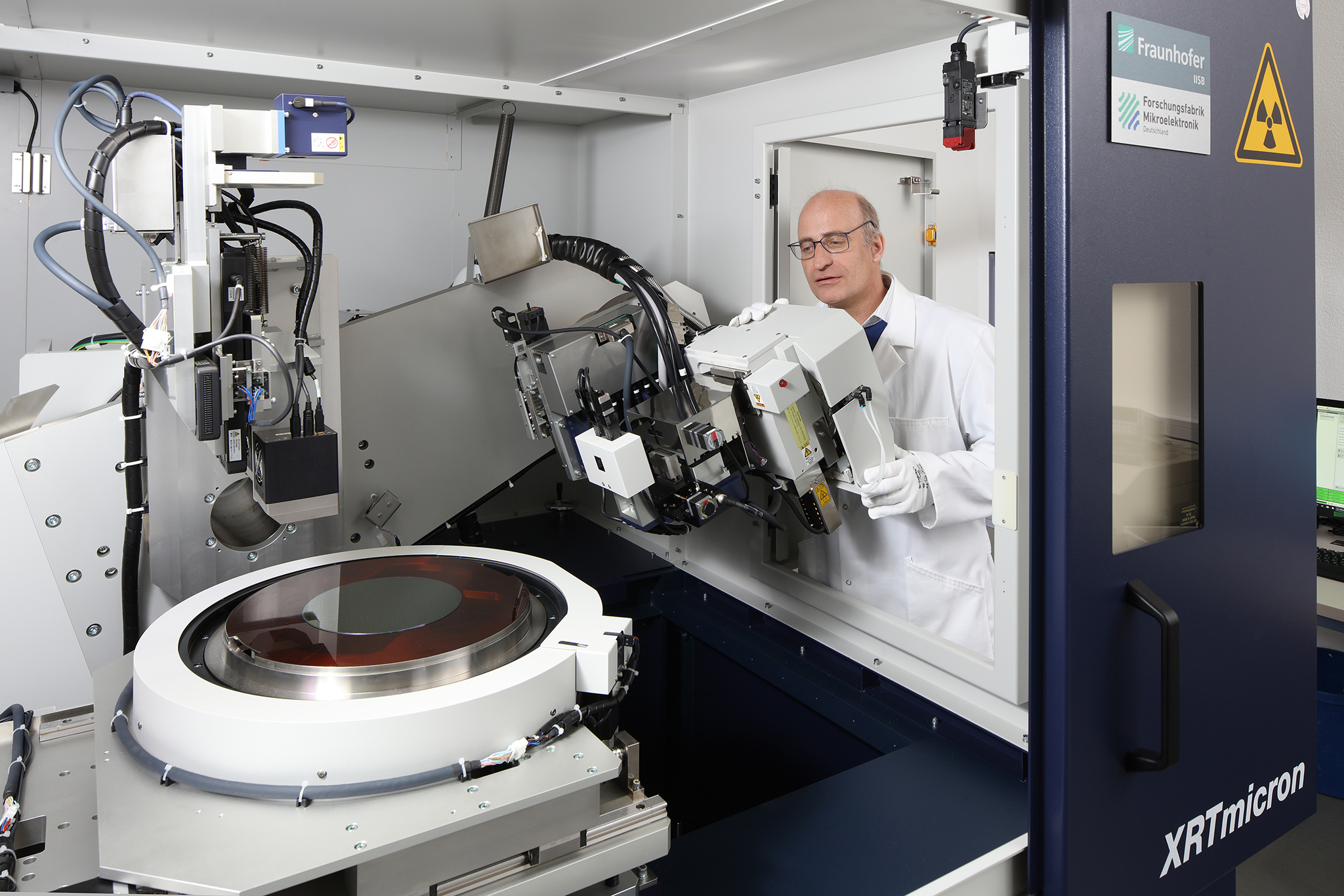
Fraunhofer IISB and Rigaku partner on wafer quality

Advanced X-ray topography tool offers more insights into semiconductor substrate and epilayer characterisation
German research institute Fraunhofer IISB and the Japanese instrumentation and analysis firm Rigaku are starting a strategic partnership in order to support the European semiconductor industry in improving and better understanding their wafer quality and yield by employing the Rigaku XRTmicron advanced X-ray topography tool.
The XRTmicron system enables investigation of crystallographic defects with high speed and highest resolution on full wafer scale. It is well suited for bare wafers, wafers with epilayer structures, partially processed wafers, as well as bonded wafers.
Rigaku has installed the latest generation X-ray topography tool, the Rigaku XRTmicron imaging system, at Fraunhofer IISB.
Michael Hippler, president at Rigaku Europe SE in Neu-Isenburg, Germany, states: “We are proud to join forces with the highly experienced team at IISB for semiconductor substrate and epilayer characterisation.”
The XRTmicron system enables investigation of crystallographic defects with high speed and highest resolution on full wafer scale. It is well suited for bare wafers, wafers with epilayer structures, partially processed wafers, as well as bonded wafers. The amount and different types of dislocations, slip lines, dislocation networks, (small angle) grain boundaries, inclusions, precipitates, pits, scratches, stress level, etc. can be imaged and quantified on the samples.
(Pictured above is an X-ray transmission topogram of the 101 reflex for a full 100 mm 4H SiC wafer and a more detailed section of the wafer.)
Two different X-ray sources – a 40kV/30mA copper source and a 50kV/24 mA molybdenum source in combination with the application of a large angle goniometer accommodate a wide range of diffraction conditions. Therefore, the XRTmicron system can be applied to different kinds of materials including semiconductors (e.g. Si, Ge, Diamond, SiC, GaN, AlN, GaAs, InP, CdTe, CdZnTe), oxides (e.g. sapphire, ruby, garnets, vanadates, niobates, quartz) and halides (e.g. fluorides, bromides).
The XRTmicron system can be operated in transmission as well as in reflection mode in order to detect defects in the volume of the sample or to quantify defects close to the surface. Furthermore, it is equipped with a standard and a high resolution XTOP CCD-camera. This leads to a spatial resolution of 5.4 µm and 2.4 µm per pixel, respectively, for a single image size of 18 mm x 13.5 mm. Full wafer mappings and detailed defect imaging of regions of interest are possible under different diffraction conditions for sample sizes of up to 300 mm in diameter. A measurement of a full 150 mm SiC wafer under the high resolution mode, for example, takes only one hour.
Additionally, the XRTmicron system is equipped with a special slit-arrangement to perform cross section topography measurements in high resolution. This gives detailed depth information through the whole thickness of the sample. For instance, it is possible to investigate whether the glide plane formation in partly processed wafers starts on the front or back side of the wafer. Furthermore, the defect formation due to epilayer growth on top of a wafer can be quantified by this feature.
Christian Reimann, group manager silicon at Fraunhofer IISB, comments: ”The XRTmicron is the only tool available in Europe so far which fulfills the requirements of highest resolution for complete wafer mappings in shortest possible time scale to analyze single crystalline materials. It is a revolution for crystallographic defect investigations compared to classical Synchrotron based topography measurements.”
Fraunhofer IISB will act as a demo centre for the XRTmicron system in Europe. Uwe Preck¬winkel, XRT product manager at Rigaku Europe SE, adds, “We already received numerous requests from the European semiconductor industry aiming to improve and better understand their product quality and yields.” It is therefore planned to standardize the operation procedures for the different costumers due to their specific needs within the strategic collaboration between Rigaku and Fraunhofer IISB.
The XRTmicron system operated at Fraunhofer IISB is part of the 'Research Fab Microelectronics Germany (FMD)' which is funded by the Federal Ministry of Education and Research. Within this Research Fab Microelectronics Germany the Fraunhofer Group for Microelectronics and two Leibniz institutes (FBH and IHP) are bundling their expertise in order to reach and expand on a new quality in research, development, and (pilot) manufacture of semiconductor-based microsystems and nanosystems.


