
New Material Pushes power Boundaries
German team to research scandium aluminium nitride (ScAlN)
Scientists from the university of Freiburg, the Sustainability Centre Freiburg and the Fraunhofer-Gesellschaft have joined forces in order to explore a new material structure that may be better suited for future power electronics.
The recently launched project 'Research of Functional Semiconductor Structures for Energy Efficient Power Electronics' (in short Power Electronics 2020+) researches the novel semiconductor material scandium aluminum nitride (ScAlN).
Oliver Ambacher, director of Fraunhofer IAF and professor of power electronics at the Department of Sustainable Systems Engineering (INATECH) of the university of Freiburg, coordinates the supra-regional collaboration.
First Components Based on ScAlN
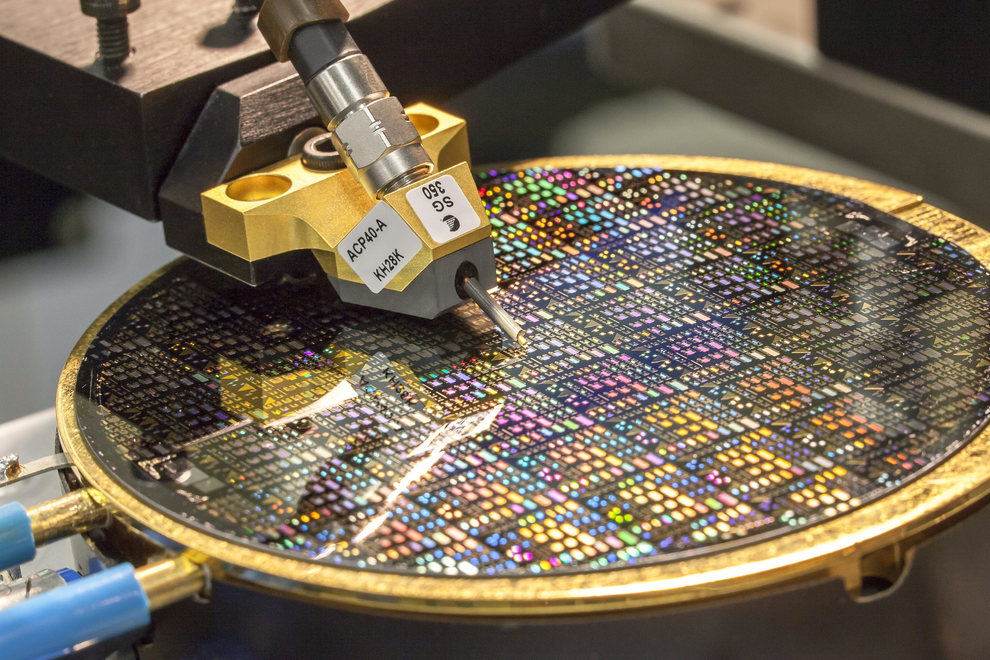
A team of researchers at Fraunhofer IAF has been working on the piezoelectric properties of ScAlN for the use in high-frequency filters for many years. ScAlN is a piezoelectric semiconductor material with a high dielectric strength which is largely unexplored worldwide with regard of its usability in microelectronic applications. "
The fact that ScAlN is especially well suited for power electronic components, due to its physical properties, has already been proven", explains Michael Mikulla, project manager on the part of Fraunhofer IAF. The aim of the project is to grow lattice-matched ScAlN on a GaN layer and to use the resulting heterostructures to process transistors with high current carrying capacity.
"Functional semiconductor structures based on materials with a large bandgap, such as ScAlN and GaN, allow for transistors with very high voltages and currents. These devices reach a higher power density per chip surface as well as higher switching speeds and higher operating temperatures. This is synonymous with lower switching losses, higher energy efficiency and more compact systems", adds Oliver Ambacher, director of Fraunhofer IAF. "By combining both materials, GaN and ScAlN, we want to double the maximal possible output power of our devices while at the same time significantly lowering the energy demand", says Mikulla.
Pioneering Work in Materials Research
One of the biggest challenges of the project is crystal growth, considering that there exsist structure neither growth recipes nor empirical values for this material, yet. The project team needs to develop these during the next months in order to reach reproducible results and to produce layer structures that can successfully be used for power electronic applications.
Specialist Collaboration and Knowledge Transfer
The research project will be conducted in close cooperation between the university of Freiburg, the Fraunhofer Institute for Applied Solid State Physics IAF, the Sustainability Centre Freiburg as well as the Fraunhofer Institure for Integrated Systems and Device Technology IISB in Erlangen, which is a member of the High-Performance Centre for Electronic Systems in Erlangen.
This new form of collaboration between university research and application-oriented development shall serve as a role model for future project cooperation. »On the one hand, this model facilitates the cooperation with companies through the prompt transfer of results from basic research to application-oriented development. On the other hand, it opens up synergies between two technically complementary Fraunhofer Centres from two different regions and thus improves both their offers for potential customers of the semiconductor industry", says Ambacher.


