
2D films that assemble themsleves
Korean team develops platform suitable for synthesising hBN and other 2D materials
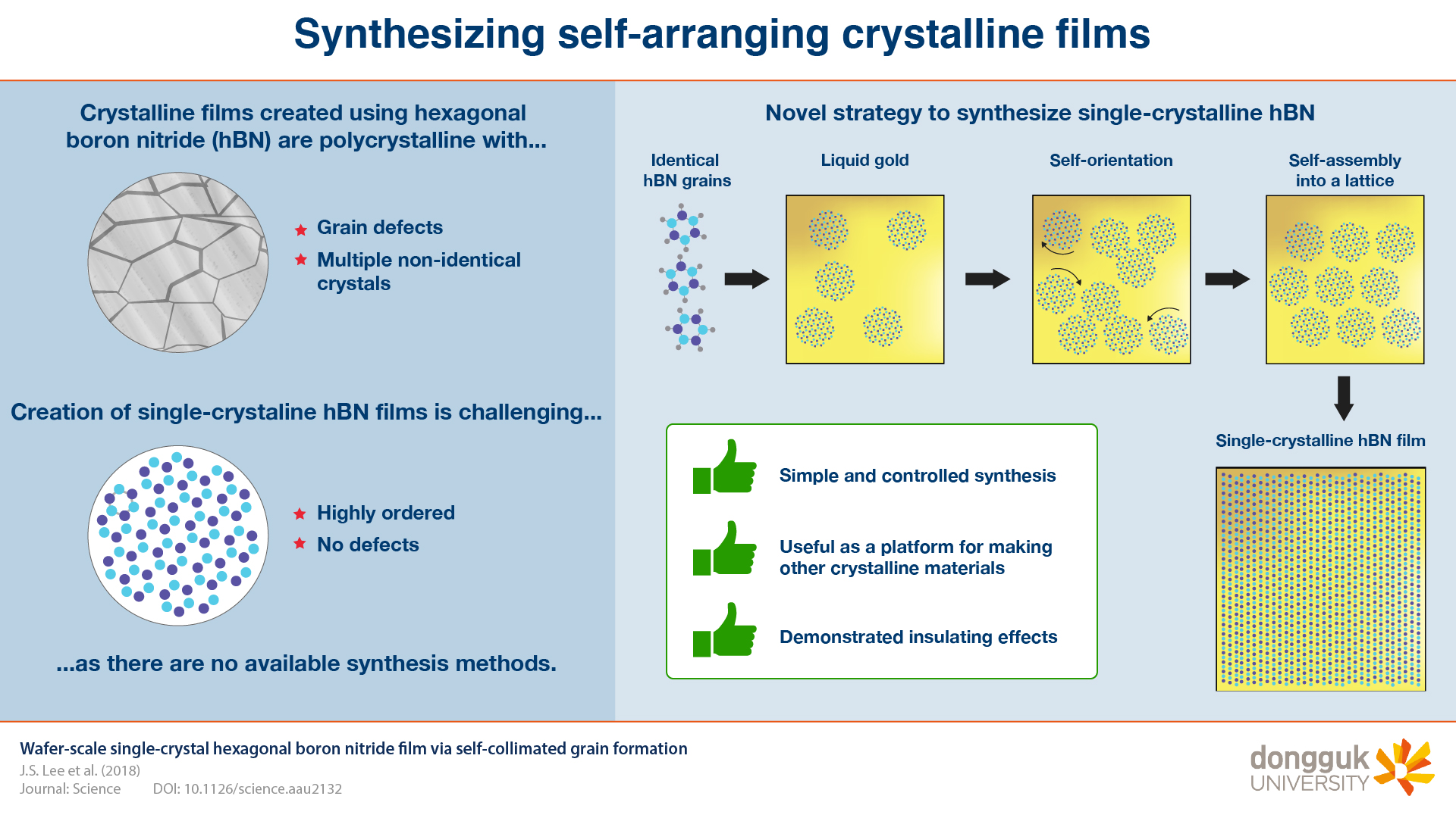
Scientists at Dongguk University (Ki Kang Kim) in collaboration with scientists from KIST (Soo Mim Kim) and Sungkyunkwan University (Young Hee Lee) have found a method for synthesising hexagonal boron nitride (hBN) films with a nearly perfect single-crystalline structure. The structure consistently self-assembles on top of liquid gold and can be used as a platform for synthesising other crystalline thin-film materials.
Their recent paper 'Wafer-scale single-crystal hexagonal boron nitride film via self-collimated grain formation' was published in the journal Science.
Crystalline structures are ideally composed of repeating identical units in a perfectly ordered fashion. As one would expect, crystals have found applications in a multitude of fields, such as optics, electronics, and chemistry, and have helped researchers understand the mechanics behind complex physical phenomena. However, synthesising perfect crystalline structures is very challenging, with most methods yielding crystals with defects or with multiple different basic units (called polycrystals).
Hexagonal BN, also called white graphite, can be synthesised in the shape of crystalline films with the width of a single atom. They have an insulating effect that has found uses in various types of scientific research. However, these films are polycrystalline and not single-crystalline. Therefore, a research team set out to find a method for synthesising single-crystalline hBN films on a small scale.
The synthesis method they developed consists of letting the thin hBN film self-assemble on top of a liquid gold substrate. Because of the surface tension of liquid gold and the characteristics of its interaction with boron and nitrogen, circular hBN grains form automatically over time. These grains grow to a specific diameter and eventually form a lattice. They can easily rotate when they are about to come into contact with another grain so as to assume the best possible orientation before joining the lattice (ref. video: https://www.youtube.com/watch?v=NI1ZhI0Qml8&feature=youtu.be)
The final product of this process is a nearly perfect single-crystalline hBN film, as the team demonstrated in many different experiments and via multiple measurements. A very promising application of such films is using them as a substrate for synthesising other crystalline thin-film materials on top of them, such as graphene. Their applications go beyond that, as Prof. Kim explains, “We demonstrated that our hBN films can serve as a protecting layer against metal oxidation and as a gas-diffusion barrier for water vapor transmission.”
This innovative synthesis method could be exploited further as well. “Our strategy for the synthesis of single-crystalline hBN films opens a new horizon for the single-crystal growth of other diatomic 2D materials,” explains Kim. This would make many single-crystalline materials easier to fabricate, allowing them to naturally find a multitude of applications.


