
G-ray Nanotech and IKZ collaborate on detector-grade GaAs wafers
Organisation to develop new platform for very high performance X-ray detectors
The Leibniz Institute for Crystal Growth (IKZ) in Berlin and G-ray Nanotech, a Swiss start-up, have entered into a research and development collaboration covering the doping of GaAs structures and the manufacturing of high purity crystals in wafer form factor for detector applications.
G-ray Industries, based in Neuchâtel, is currently developing ultra-high performance detectors dedicated to industrial non-destructive testing solutions. These ultra-high-performance detectors are developed in partnership with CSEM (the Swiss Centre for Electronics and Microtechnology) based on G-ray's patented latenium technology.
the latenium architecture is based on covalent low-temperature semiconductor bonding between the absorber and the readout wafers a specific combination of semiconductor alloy grown by epitaxy that defines the sensitivity of the absorption layer.
"We are delighted to work with a world-leading institute in the field of material sciences," says Philippe Le Corre, CEO of G-ray Nanotech. "The competencies of IKZ will allow us to accelerate significantly the expansion of our latenium detector architecture into medium-large energy X-rays applications as well as in the infra-red spectrum."
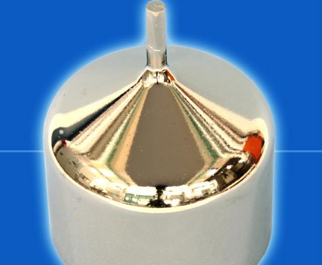
The latenium Evaluation kits are available for evaluation purposes as of Q1-2019. In addition, the G-ray technologies - in particular the covalent bonding of a silicon wafer to a GaAs, Ge or Si wafer at low temperatures and the very fast epitaxial growth of Germanium structures - are being positioned in the fields of high-energy physics research for new particle detectors and in vision systems for the automotive industry. The picture above shows GaAs-single crystal 4, grown by the VGF (Vertical gradient freeze) method.
"We are pleased to start a long-term collaboration with G-ray Industries," says Thomas Schroeder, IKZ´s scientific director. "IKZ is committed to push high performance crystalline materials to market applications and the state-of-the-art X-ray imaging detector development at G-Ray is a nice opportunity for us. We consider 3D heterointegration via bonding approaches as a fruitful strategy for us to innovate technologies by high quality, precisely tailored crystalline materials."
"With our expertise in materials science and technology we have supported the G-ray team right from the start. This is an outstanding opportunity to bring a ground-breaking X-ray detector technology to the market," says Gian-Luca Bona, CEO of Empa, the Swiss Federal Laboratories for Material Science and Technology.


