
Making microLEDs on 200 mm silicon
Armed with minimal wafer bow, good wavelength uniformity and an internal quantum efficiency exceeding 80 percent, the 200 mm GaN-on-silicon epiwafer is an ideal ingredient for making displays BY Liyang Zhang, Kai Liu, Peng Xiang, Hongjing Huo, Ni Yin and Kai Cheng FROM ENKRIS SEMICONDUCTORS
Flaws hamper the two incumbent display technologies, which are based on liquid crystals and organic LEDs. Those that feature liquid crystals are compromised by the complex architecture: each individual sub-pixel consists of a backlight, polarizers, a matrix of liquid crystal, and colour filters. This leads to a low efficiency. With OLEDs, efficiency is addressed, but at the expense of lifetime and reliability.
A far more promising option for making a display is an array of microLEDs. Each of its pixels is formed with an LED with dimensions of less than 30 mm that has the strengths of its bigger brother. Those merits include a high brightness and contrast ratio, a low power consumption, a fast response time, a long lifetime, a wide range of operating temperature and a wide viewing angle.
Armed with all these attributes, the power consumption of a microLED is very low. It’s just 10 percent of that of a liquid crystal display, and half of that of one based on OLEDs. The low power consumption does not hold back the brightness of the microLED display: it can be as bright as that made from OLEDs, while using just one-tenth of the OLED’s emitting area.
On top of all these strengths, gains may be realised from the smaller pixel size. This makes microLEDs an excellent candidate for transparent display applications – and it opens the door to integrating, in the spare space between the emitters, sensors and circuits. Adopting this approach enables the construction of displays with embedded sensing capabilities, such as fingerprint identification.
Thanks to the remarkable set of properties listed above, the microLED can be used in many applications, including large TVs, smart watches and wearables, virtual reality and automotive head-up displays. Consequently, the microLED display is regarded as a leader of next-generation display technology.
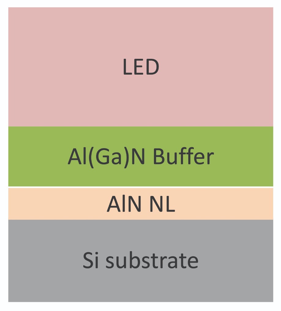
Figure 1. An LED epistructure used by Enkris for making devices on 200 mm silicon.
Manufacturing options
There are two options for fabricating microLEDs: monolithic integration and mass transfer. For applications like wearables that have less than 1000 pixels per inch, the ‘pick-and-place’ approach is used for massively parallel transfer. However, when microLEDs are used to make high-resolution displays – that is those that have more than 1,000 pixels per inch – pick-and-place is not feasible. In this case, the monolithic integration of arrays is a better approach to producing high-resolution displays, because it can directly transfer a processed LED wafer to a target backplane through wafer-bonding technology.
For this latter approach, production ideally involves the use of large, flat epi-wafers with a narrow wavelength bin range and a low defect level. Flatness is important, because it allows the epiwafer to be transferred directly to a target backplane through wafer-bonding technology. A narrow spread of wavelengths is highly advantageous, because it can eliminate time-consuming die binning; and a low defect level is critical to improving final yield.
Requirements for the epiwafer may be specified as follows: a wafer diameter of at least 150 mm, to ensure high transfer efficiency; a wafer bow below 30 mm, to enable a high bonding yield; a wavelength uniformity that places die in a ±1 nm bin, so that display production is binning free; and a combination of a high internal quantum efficiency and a high light extraction efficiency, ensuring high brightness.
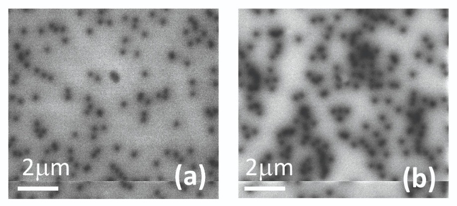
Figure 2. Cathodoluminescence reveals the threading dislocation density of unintentionally doped GaN on a (a) 200 mm silicon substrate and a (b) 100 mm planar sapphire substrate. Densities of threading dislocations are estimated to be 1.5 x 108 cm-2 and 1.9 x 108 cm-2 for (a) and (b), respectively.
The silicon solution
At Enkris Semiconductor, China, we believe that the best way to fulfil all of these requirement is to produce LED epiwafers on silicon substrates. That’s because silicon is available in sizes of up to 300 mm in diameter, cost is low – it is less than $50 for a 200 mm substrate – and this material can provide the foundation for epiwafers with a high quality and a low particle level. What’s more, GaN-on-silicon offers the advantages of compatibility with mature silicon-based manufacturing, which has well-established technologies for thin-film processes and the monolithic integration of arrays. And last but by no means least, proper strain engineering can be applied to GaN-on-silicon epiwafers, leading to good uniformity and minimal bow.
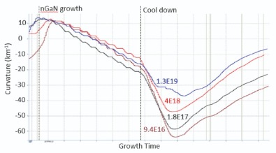
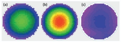
Figure 3. In-situ wafer curvature measured during the growth of the silicon-doped GaN step. Different doping concentrations are indicated in each curve.
Figure 4. Wafer bow map for three different types of LED epiwafer: (a) 100 mm GaN-on-sapphire LED, (b) 150 mm GaN-on-sapphire LED, and (c) 200 mm GaN-on-silicon.
To produce our LED epiwafers, we load 200 mm silicon substrates into an MOCVD chamber and grow a stack of nitride layers. The growth process is not straightforward. It is impossible to grow GaN directly on a silicon substrate, due to ‘melt-back etching’, which is a high-temperature reaction of gallium and silicon to form a gallium-silicon eutectic at high growth temperatures. The solution is to deposit an AlN nucleation layer prior to GaN growth. After this, an Al(Ga)N strain management buffer layer is added, followed by a standard LED structure.
We have scrutinised our epiwafers with XRD rocking-curve scans and cathodoluminescence measurements. These techniques highlight the high crystalline quality of our material. Full-width at half-maxima for rocking curves in the (002) and (102) directions are 334 arc sec and 299 arc sec, respectively. These values correspond to a threading dislocation density of around 1.5 x 108 cm-2 (see Figure 2 (a)). In comparison, for GaN epilayers on a planar sapphire, this figure is around 1.9 x 108 cm-2 (see Figure 2 (b)).
Another key requirement for LED epiwafers is heavily silicon-doped n-GaN. This is tricky to deposit, as it can lead to the relaxation of compressive stress, via the creation of threading dislocation inclination in the presence of high-density threading dislocations.
We have measured the in-situ curvature of our GaN-on-silicon wafers during the growth of n-type layers with different doping concentrations (see Figure 3). Plotting curvature as a function of doping produces a straight line, even for doping levels in excess of 1 x 1019 cm-3, indicating minimum compressive stress relaxation. This has been accomplished by reducing the dislocation density, which in turn minimises compressive stress relaxation.
It is preferable to produce thin epi-layers for microLEDs, because they result in a small wafer bow and a higher bonding yield. We are able to do just that, producing wafers with a total epiwafer thickness below 3.5 mm and thickness uniformity of just 1.5 percent.
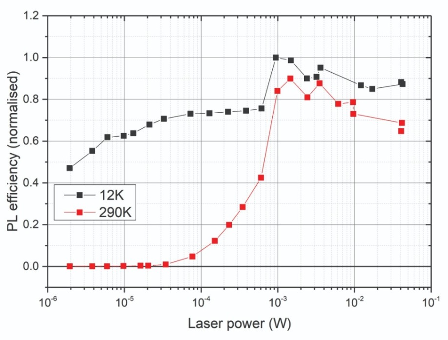
Figure 5. Measurements of quantum efficiency, as function of excitation power density, for a 200 mm GaN-on-silicon LED epiwafer held at 12K and 290K. These plots indicate that the internal quantum efficiency for this heterostructure is more than 80 percent.
A key requirement for wafer bonding is minimal wafer bow, because this allows the use of stepper lithography systems and wafer mass transfer. For conventional GaN-on-sapphire, epilayers stress is primarily determined by thermal mismatch – left unchecked, it leads to a large convex bow. Typical values for wafer bow for 100 mm and 150 mm GaN-on-sapphire LED wafers are 120 µm and 170 µm, respectively (see Figures 4 (a) and (b)). However, for our 200 mm GaN-on-silicon, proper stress engineering ensures a final wafer bow of less than 30 mm (see Figure 4 (c)).
When the size of the LED chip is shrunk to mini or micro dimensions, surface texturing cannot be used to improve light extraction. Making matters worse, sidewall non-recombination becomes more severe. For these classes of LEDs, the key is a high internal quantum efficiency. Our wafers meet this requirement, with an internal quantum efficiency estimated to exceed 80 percent (see Figure 5 for temperature and power dependent photoluminescence measurements of our GaN-on-silicon LED wafer).
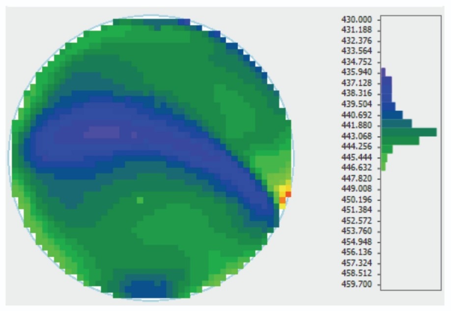
Figure 6. (a) Mapping the average dominant wavelength for a 200 mm GaN-on-silicon LED reveals an average wavelength of 442 nm and a standard deviation of 2.4 nm. (b) Corresponding probability plot of the average dominant wavelength.
One of the hallmarks of our epiwafers is their tremendous uniformity, underscored by photoluminescence mapping. This technique reveals that the average dominant wavelength is 442 nm, and the standard deviation is as low as 2.4 nm (see Figure 6 (a)). Thanks to this high degree of uniformity, 99 percent of the wafer falls within a 7 nm wavelength bin range (see Figure 6 (b)).
We believe even better results are possible. To realise superior wavelength uniformity, we will undertake further optimization, engineering wafer bow during the growth of the multi-quantum wells to match the profiled susceptor. This will enable uniform multi-quantum-well temperatures across the whole wafer during growth.
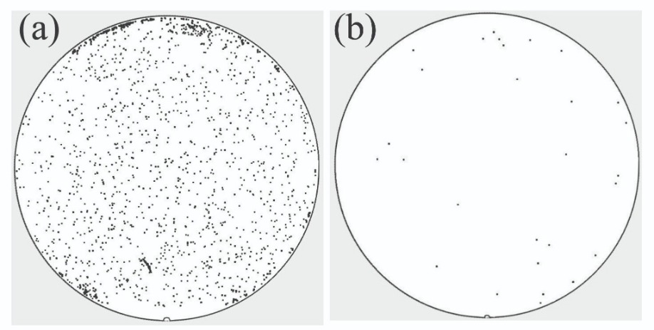
Figure 7. Defect inspection reveals the far higher particle count for 150 mm sapphire (a) than (b) 200 mm silicon. (c) The particle count of two different substrates.
A little-known benefit of silicon substrates, rather than those made from sapphire, is a far lower particle level. For 150 mm sapphire, due to the non-mature chemical mechanical cleaning process and the cleaning steps that follow, the particle level is typically around 2000 (see Figure 7). In comparison, for 200 mm silicon, the particle level may be consistently controlled below 100. As particles are embedded in the surface during growth and impair material quality, the fewer there are, the better the epiwafers (see Figure 8 for an example of the particle count for a GaN-on-silicon epiwafer).
One of the potential downsides with GaN-on-silicon epiwafers is cracking at the edge of the material, due to strain. However, we are able to control cracks, limiting their propagation to within 1.5 mm of the wafer edge. Note that even without any edge exclusion, the total number of cracks across the entire wafer is less than 100.
The extensive characterisation of our epiwafers highlights their great capability for making microLEDs. Armed with a wafer bow below 30 µm, an internal quantum efficiency of more than 80 percent and good wavelength uniformity, our material is well set for supporting the ramp in the manufacture of microLED displays.
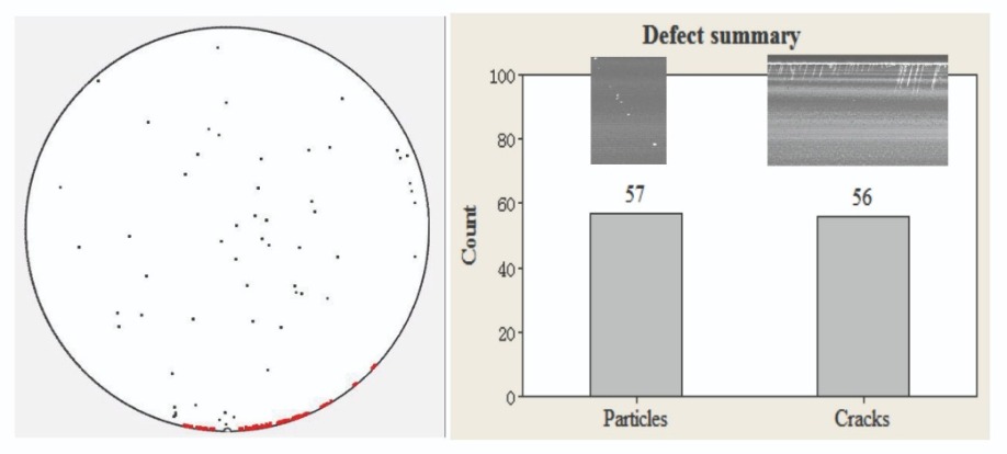
Figure 8. Defect inspection highlights the high-quality of 200 mm GaN-on-silicon LED epiwafers produced by Enkris
This work is partially supported by grant from the Natural Science Foundation for Young Scientists of Jiangsu Province (Grant No. BK20160376).


