
Changing the electronic properties of 2D materials
Swiss team combins different naturally occurring patterns to create new synthetic materials
Combining atomically thin layers of graphene and the compound semiconductor boron nitride (BN)at a slightly rotated angle changes their electrical properties. Physicists at the University of Basel have now shown for the first time the combination with a third layer can result in new material properties also in a three-layer sandwich of carbon and BN. This significantly increases the number of potential synthetic materials, report the researchers in the scientific journal Nano Letters.
Last year, researchers in the US caused a big stir when they showed that rotating two stacked graphene layers by a 'magical' angle of 1.1 degrees turns graphene superconducting - a striking example of how the combination of atomically thin materials can produce completely new electrical properties.
Scientists from the Swiss Nanoscience Institute and the Department of Physics at the University of Basel have now taken this concept one step further. They placed a layer of graphene between two BN layers, which is often serves to protect the sensitive carbon structure. Doing so, they aligned the layers very precisely with the crystal lattice of the graphene.
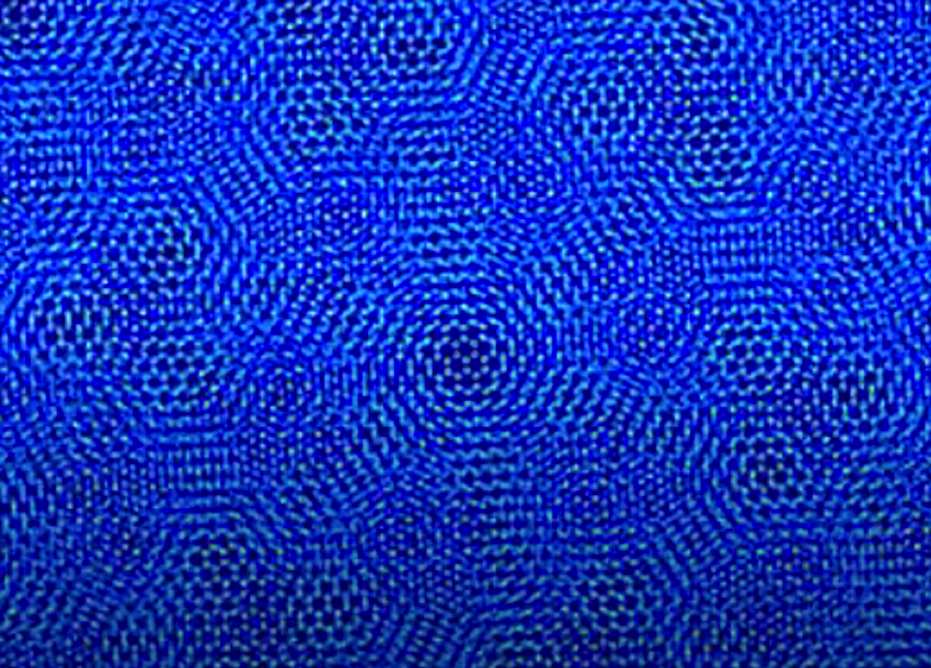
The effect observed by the physicists in Christian Schönenberger's team is commonly known as a moiré pattern: when two regular patterns are superimposed, a new pattern results with a larger periodic lattice.
Lujun Wang, a member of the SNI PhD School and researcher in Schönenberger's team, also observed effects of this kind of superlattice when he combined layers of BN and graphene. The atoms are arranged hexagonally in all layers. If they are stacked on top of each other, larger regular patterns emerge, with a size depending on the angle between the layers.
It had already been shown that this works with a two-layer combination of graphene and BN, but the effects due to a second BN layer had not yet been found.
When the physicists from Basel experimented with three layers, two superlattices were formed between the graphene and the upper and the lower boron nitride layer, respectively. The superposition of all three layers created an even larger superstructure than possible with only one layer.
Scientists are very interested in these types of synthetic materials, since the different moiré patterns can be used to change or artificially produce new electronic material properties.
"To put it simply, the atomic patterns determine the behaviour of electrons in a material, and we are combining different naturally occurring patterns to create new synthetic materials," explains Andreas Baumgartner, who supervised the project. "Now we have discovered effects in these tailor-made electronic devices that are consistent with a three-layer superstructure," he adds.


