

Drawing the heat with Diamond

Sucking the heat out of a GaN transistor with diamond film is to become ever more common, thanks to a strengthening supply chain for this technology
RICHARD STEVENSON REPORTS
Diamond has many fine attributes. It is renowned for its brilliance, which makes it a very fine choice for making jewellery; and it is blessed with great hardness, allowing it to be used in tools for cutting, drilling and sawing, and on the tip of cantilevers, to trace the modulations in vinyl records.
Lesser known, but equally exceptional, is diamond’s thermal conductivity. Thanks to strong covalent bonds and low phonon scattering, its conductivity is around 2000 W m-1 K-1, a value five times that of copper.
This incredibly high conductivity has piqued the interest of the electronic community, which has been investigating diamond’s capability for extracting the heat out of a GaN HEMT. Efforts in this direction can be traced back to 2003, with the first successful attempt to produce a GaN-on-diamond structure. Milestones since then include the first GaN-on-diamond transistor in 2006, and DARPA’s Near Junction Thermal Transport (NJTT) programme, kicked off in 2011, that has aided the development of this technology.
Recently, further strides have been made that put in place the groundwork to support the commercialisation of GaN-on-diamond technology. Several companies are now playing a significant
role in this fledgling industry, with many in attendance at Diamond D-day, a one day conference held in Bristol, UK, towards the end of January. Those at this gathering, organised by Martin Kuball from the University of Bristol, included suppliers of tools for depositing diamond, providers of GaN-on-diamond epiwafers and foundry services, and makers of devices.
Up in space
One of the pioneers of the GaN-on-diamond HEMT is Akash Systems. This outfit, based in San Francisco, CA, devotes its efforts to developing small satellites, satellite transmitters, and the RF power amplifiers that serve them.
Speaking on behalf of Akash, the company’s vice president of materials, Daniel Francis, began his talk by claiming that diamond is a satellite’s best friend. He argued that the addition of a diamond foundation produces a three-fold hike in power density, and a considerable reduction in operating temperature. He cited work by the Air Force Research Laboratory, showing that the addition of a diamond layer reduced the channel temperature by between 40 percent and 50 percent, compared with GaN-on-silicon and GaN-on-SiC devices.
That reduction is a big deal. Note that the rays of the sun can propel satellite temperatures to as high 180 °C – and radiation is the only option for dissipating heat, so it is crucial to get as much of it as possible out of the device.
Akash is producing its GaN-on-diamond devices from 4-inch wafers. “If it’s not full wafer, it’s not production,” said Francis.
He outlined three potential options for forming GaN-on-diamond structures. One is to grow GaN layers directly on diamond, but this requires the use of intermediate layers, and is ruled out by the relatively small the size of the diamond substrate. Another option is bonding, but a ‘glue’ is needed to bond the GaN and the diamond. Amorphous SiN is a popular choice, but it has a thermal conductivity of just 1 W m-1 K-1, compromising the benefits of the diamond layer.
The third way, pursued by Akash, is to grow diamond on GaN-based epistructures. Engineers at the west-coast firm start with GaN-on-silicon epiwafers with a SiN transition layer – it is less than 35 nm-thick, has a conductivity of around 10 W m-1 K-1, and provides a good dielectric interface. Fabrication of devices involves separating the epilayers from the silicon substrate.
Efforts associated with improving production have led to a greater consistency associated with removal of the AlGaN buffer, better control of the thickness of the adhesion layer – it is now controlled to within 5 nm – and a reduction in wafer bow to less than 20 µm.
Engineers target a thickness for the diamond layer of 125 mm. To ensure that they realise this, they deposit more material, and then apply a polishing step to thin the diamond to the required thickness.
Francis revealed that when the growth of diamond begins, it can create nanocrystals, which have a low thermal conductivity. But as growth continues, grains get larger, increasing thermal conductivity.
Capacitance-voltage measurements on the processed wafers reveal a “low, flat capacitance”. This is attributed to low interface charging. Plots are much closer to those for GaN-on-SiC, than for GaN-on-silicon.
Results on recent multi-finger devices reveal a power-added efficiency of around 60 percent. According to Francis, this figure is comparable to that of standard devices operating at 10 GHz.
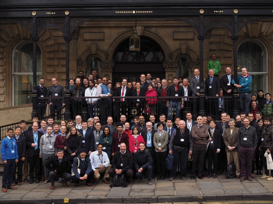
The Diamond D-day conference, held at the Bristol Mari ot Hotel, attracted 120 delegates. About half of those that attended came from overseas.
GaN-on-diamond epiwafers
If developers of GaN-on-diamond devices prefer to start their fabrication work with epiwafers of this material, they have the option of buying 4-inch material from RFHIC.
At Diamond D-Day, RFHIC’s Director and General Manager, US, Won Sang Lee, began his presentation by claiming that the market for epiwafers of GaN-on-SiC HEMTs is “strong”. But he believes that GaN-on-diamond will be “the next step”.
RFHIC wants to be the pioneer of the GaN-on-diamond semiconductor industry. It is well-placed, having 63 patents associated with this technology, and exclusive intellectual property that is said to cover everything except the commercial satellite sector. The company has identified several potential markets for GaN-on-diamond, including self-driving cars, military radar, and industrial, medical and scientific sectors.
Lee compared what he considers to be the three main technologies for RF, high-power devices: silicon LDMOS, GaN-on-SiC, and GaN-on-diamond. He argued that the it is only the latter that is capable of providing operating frequencies up to 100 GHz, making it the leading candidate for the future.
He predicts that the success of GaN-on-diamond will begin with deployment in 5G base stations. The merits of this material combination are not limited to a substantial power density, but also include: greater linearity, stemming from superior carrier transport; and better reliability, due to the lower operating temperature of the chip.
RHFIC, which started developing its GaN-on-diamond technology back in 2015, is now capable of producing GaN-on-diamond material in substantial volumes in Korea, and in smaller quantities at its R&D facility in the US. The plan is to start shipping engineering samples to its customers in the second quarter of this year.
Goals for the future include increasing the production quantity of GaN-on-diamond to 100 epiwafers per month, optimising device layers to improve performance, and increasing yield – currently it’s just 40 percent.

As the small satellite space race takes off, Akash Systems is set to send GaN-on-diamond systems into orbit.
Device foundry
One company with the capability to process RHFIC’s GaN-on-diamond epiwafers into devices is compound semiconductor foundry service provider GCS. In Bristol Daniel Hou, a spokesman for the company, detailed some of the challenges and the rewards of this approach.
A downside is that in an automated fab, some tools may be unable to handle these epiwafers. This can be caused by tensile strain in the material, leading to a wafer bow of up to a few millimetres. Such a distortion can wreak havoc with printing processes for i-line steppers. The solution, explained Hou, is to choose a carrier with the right coefficient of thermal expansion. Using a combination of a perforated SiC carrier, dry and wet etching steps, thermal release tape bonding and high-temperature polymer bonding, bow can be slashed to just 20 µm.
Hou revealed that another issue is that the implant isolation step can lead to a “huge” leakage current. It rockets by six orders of magnitude.
The engineers at GCS address this hike with an additional step for treating the surface. This results in DC characteristics that are similar to those for GaN-on-silicon: maximum current is 1 A/mm, peak transconductance is 250 mS/mm, breakdown voltage exceeds 100 V, and the on-off ratio is in excess of 106.
RF measurement on these devices are encouraging. Applying a 10 percent duty cycle to 0.65 µm HEMT, and cranking up the voltage from 50 V to 100 V, produces an increase in the power density at 2 GHz from 15.5 W/mm to 22.5 W/mm.
Efforts at GCS have also been directed at developing a through-substrate via process. This involves: laser drilling from the frontside; plating with gold to partially fill the via; sputtering a seed metal; and then gold plating, both on the front side and the back side.
Multi-finger devices made with this process are capable of producing an output of 11.2 W, and 15-19 dB of gain. Hou describes these results as “respectable”, and says they provide proof that the via process is “working”.
An all-diamond device
With a bandgap of 5.45 eV – that is even higher than that of gallium oxide – diamond can also be viewed as a promising material for making high-power devices.
Some of the results obtained with diamond devices were briefly discussed in a talk given by Andrew Barnes from the European Space Agency. He mentioned transistors with a maximum oscillation frequency of 20 GHz, and a cut-off frequency of about 7.7 GHz. This enabled up to 22 dB of gain, a result Barnes described as “quite encouraging”.
However, he warned the audience that diamond has its drawbacks, including being very expensive, and very difficult to dope.
An even stronger case for steering clear of diamond devices came from Oliver Williams from Cardiff University, who said: “I did my PhD on diamond devices and it didn’t go well.” In his view, n-type doping doesn’t work, and the diameter of the native substrate is stuck at half an inch, despite promises dating back two decades that 1-inch material is just around the corner.
So, based on the presentations at Diamond D-day, it is best to restrict diamond’s role within the compound semiconductor industry to extracting the heat out of the GaN HEMT. Used for this, it can do a great job. And with a strengthening supply chain taking place, there is a good chance that GaN-on-diamond devices will start to see widespread in space, along with increasing deployment in applications far nearer to home.


