
NIST team boosts intensity of GaN nanowire LEDs
UV LEDs produce five times higher light intensity thanks to a bit of aluminium
Nanowire gurus at the National Institute of Standards and Technology (NIST) have made ultraviolet LEDs that, thanks to a special type of shell, produce five times higher light intensity than do comparable LEDs based on a simpler shell design.
Ultraviolet LEDs are used in a growing number of applications such as polymer curing, water purification and medical disinfection. Micro-LEDs are also of interest for visual displays. NIST staff are experimenting with nanowire-based LEDs for scanning-probe tips intended for electronics and biology applications.
The new, brighter LEDs are an outcome of NIST's expertise in making high-quality GaN nanowires. Lately, researchers have been experimenting with nanowire cores made of silicon-doped GaN, which has extra electrons, surrounded by shells made of magnesium-doped GaN, which has a surplus of holes for missing electrons.
The NIST group previously demonstrated LEDs that produced light attributed to electrons injected into the shell layer to recombine with holes. The new LEDs have a tiny bit of aluminum added to the shell layer, which reduces losses from electron overflow and light reabsorption.
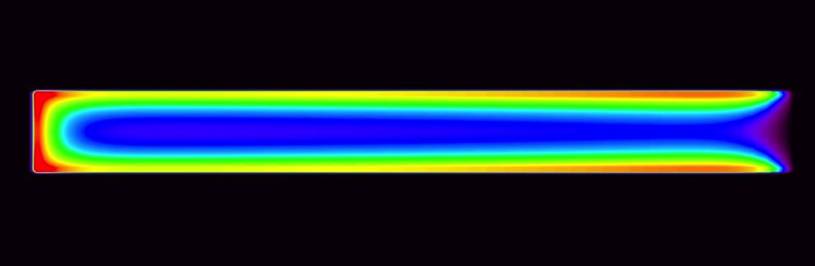
As described in the journal Nanotechnology, the brighter LEDs are fabricated from nanowires with a p-i-n structure, a tri-layer design that injects electrons and holes into the nanowire. The addition of aluminum to the shell helps confine electrons to the nanowire core, boosting the electroluminescence fivefold.
"The role of the aluminum is to introduce an asymmetry in the electrical current that prevents electrons from flowing into the shell layer, which would reduce efficiency, and instead confines electrons and holes to the nanowire core," first author Matt Brubaker said.
The nanowire test structures were about 440 nm long with a shell thickness of about 40 nm. The final LEDs, including the shells, were almost 10 times larger. Researchers found that the amount of aluminum incorporated into fabricated structures depends on nanowire diameter.
Group leader Kris Bertness said at least two companies are developing micro-LEDs based on nanowires, and NIST has a Cooperative Research and Development Agreement with one of them to develop dopant and structural characterisation methods. The researchers have had preliminary discussions with scanning-probe companies about using NIST LEDs in their probe tips, and NIST plans to demonstrate prototype LED tools soon.
The NIST team holds US Patent 8,484,756 on an instrument that combines microwave scanning probe microscopy with an LED for nondestructive, contactless testing of material quality for important semiconductor nanostructures such as transistor channels and individual grains in solar cells. The probe could also be used for biological research on protein unfolding and cell structure.
'UV LEDs Based on p-i-n Core-Shell AlGaN/GaN Nanowire Heterostructures Grown by N-polar Selective Area Epitaxy' by M.D. Brubaker et al; Nanotechnology, March 21, 2019.


