
Equipping MBE with artificial intelligence
Monitoring electron diffraction with artificial intelligence promises to boost epiwafer production yields
BY Young-Kyun NOH FROM IVWorks
We are in the midst of the Fourth Industrial Revolution. Innovation in manufacturing is underway, thanks to integration of conventional production and network connectivity with the Internet of Things (IoT) and Artificial Intelligence (AI). The benefit of this is that it enables AI manufacturing – that is, the use of production processes that are managed through intelligent machines, systems, and networks that autonomously sense and analyse information.
The adoption of AI and IoT is already driving big changes within a range of industries. Armed with AI, manufacturing processes can be monitored in real-time through the sensing, collecting, and analysing of sensor data using IoT. This capability allows the swift identification and resolution of problems in manufacturing facilities, leading to enhanced productivity. Ultimately, it will enable many tasks to be transferred from human engineers to AI systems, and create a seamless manufacturing environment.
At IVWorks, a GaN epiwafer foundry start-up headquartered in Daejeon, South Korea, we are moving with the times. We have developed and applied a deep learning-based AI epitaxy platform, known as Domm, that dramatically improves the productivity and scalability of MBE-grown epiwafers. This patented technology, which uses a deep learning algorithm to detect and analysis electron diffraction patterns, monitors crystal growth at the atomic level in real time.
Today, we are using our Domm platform on three MBE systems that produce 100 mm to 200 mm GaN epiwafers for DC and RF power devices. We monitor the electron diffraction pattern with a deep learning algorithm, and information about the entire crystal structure of the epiwafer is classified and converted into data. If abnormal patterns are identified, an alarm is raised with the engineer. This level of adoption of AI is referred to as Level 2 (see Figure 1 for an overview of the different levels).
This is just the start of our venture into AI. In February 2019, we closed a $6.1 million series B funding round that will enable us to expand our manufacturing capabilities and upgrade the Domm platform to higher levels (see Figure 2 for our roadmap). The first step will be a move to Level 3, the AI Assistance level. Here, data acquired through the deep learning algorithm is learned by correlating it with the quality data of the produced epiwafers. This allows the probability of pass/fail to be intelligently predicted in real time, assisting the engineer.
Further ahead, we will move to Level 4 and then on to Level 5. The lower of these is known as the AI Production level. This bolsters yield by automatically revising the process conditions of the recipe in real time, according to the predicted probability of pass/fail. When operating at Level 5, known as the AI Manufacturing level, it is possible for AI to develop a customized epiwafer recipe of a new structure. To accomplish this, epiwafer quality results, according to recipes, are accumulated and learned. In addition, correlations are established, and their validity analysed.
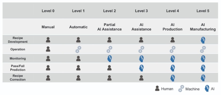
Figure 1. Various levels for IVWorks Domm platform.
The need for AI
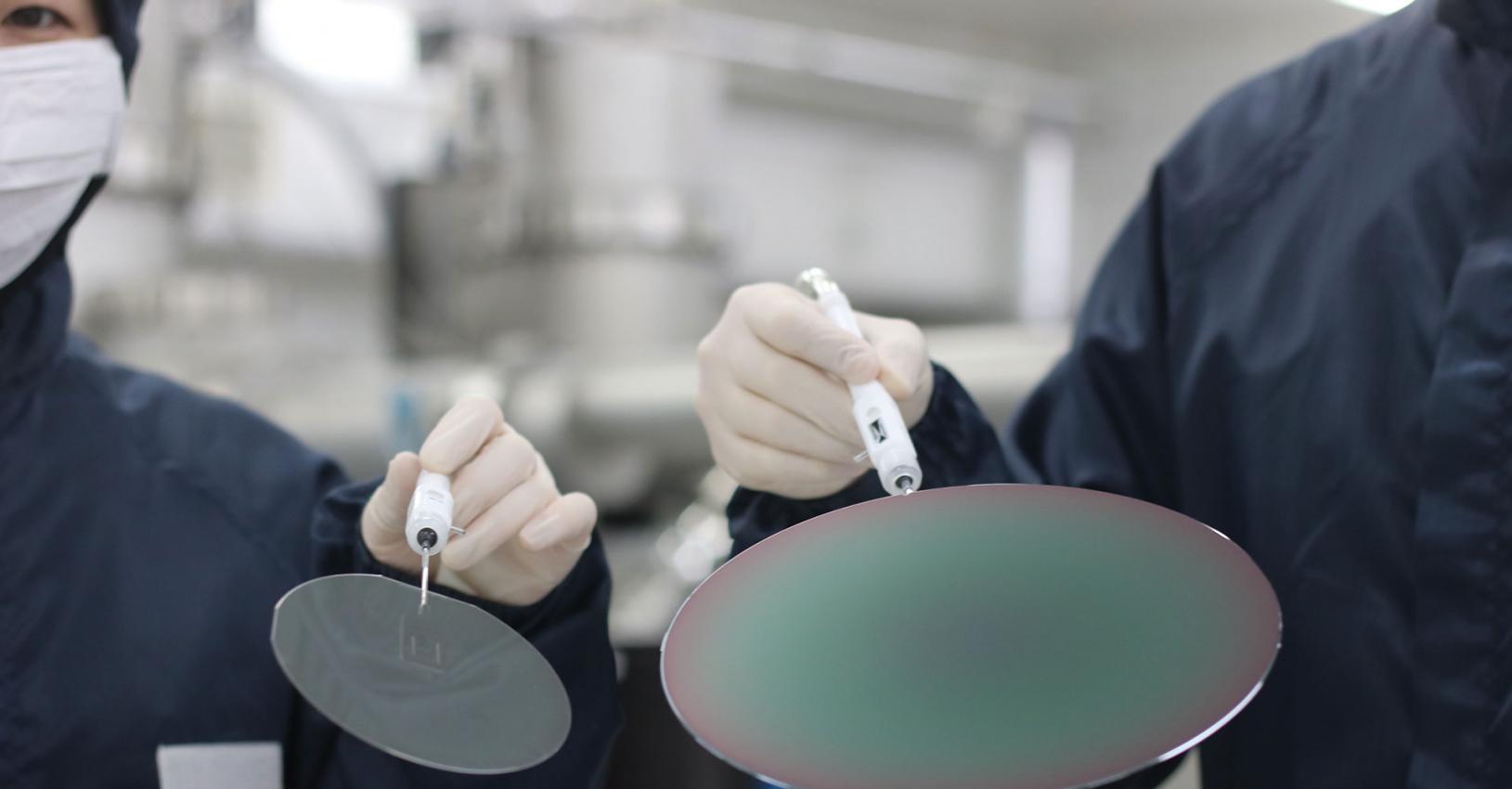
The use of AI makes a dramatic impact on MBE, due to the complexity of this growth process. Successful growth of epiwafers demands strict control of many conditions, including: the substrate temperature; the temperature distribution of the substrate and the reactor; the internal pressure inside the reactor; the number of source atoms; the relative ratio between the sources; the growth rate; the size and geometry of the reactor; the flow pattern and the flux pattern of the source; and atomic migration (or diffusion), which includes binding reactions on a substrate surface. To illustrate this complexity, just consider the growth of a 3 µm-thick GaN FET epiwafer. It is formed by depositing approximately 12,000 or more atomic layers, each added with precisely controlled conditions (see Figure 3).
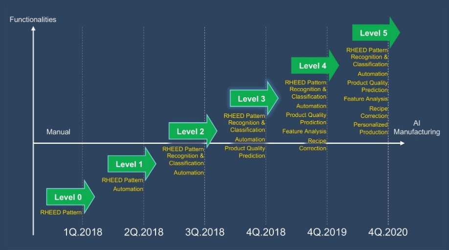
Figure 2. Roadmap for IVWorks Domm platform.
So complex is the growth process that two nominally identical models of the same state-of-the-art MBE reactor have different optimum conditions. And maintaining the conditions in either of them is far from easy – it takes an engineer with significant expertise to secure and maintain reproducibility that satisfies pass/fail tolerance for target characteristics, even when the same recipe is being used on the same reactor, run after run after run.The conventional approach to managing productivity is for an engineer to collect and analyse data related to the epitaxial growth process conditions, the equipment status, and the results associated with the quality of the manufactured epiwafers. However, comprehensive analysis of the epi-structure and the process are challenging, and this can lead to variations in the analysis of the collected data, depending on the expertise of the engineer. When the collected data is difficult to quantify, variations are exacerbated, compromising the reliability of the results of the analysis, and ultimately hampering efforts to control and monitor the epiwafer manufacturing process. Since limits on human resources often cause bottlenecks in productivity and scalability, there is a great demand for a highly advanced, automated solution that is efficient, convenient, and capable of a real-time, seamless response that maximises the manufacturing productivity of the epiwafers.
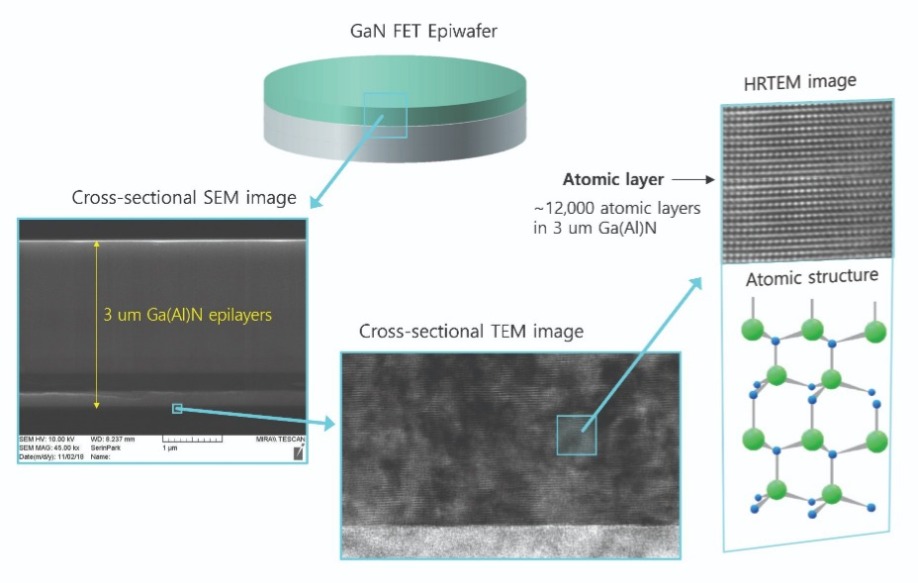
Figure 3. The epiwafer is single crystalline semiconductor wafer upon which complex structures, comprising many individual atomic layers, are deposited.
Gaining the edge with AITo develop automated solutions that maximise epiwafer manufacturing productivity, it is critical to employ quantitative monitoring of both the process state of the equipment and the growth state of the epi-structure. Given that the focus has to be on maximising the yield of products and managing the manufacturing process to ensure that the material is as close as it can be to the target characteristics, process conditions should be ideally corrected in real-time during epitaxial growth. And if that’s not possible, the recipe must be updated after every growth.
Automation of the monitoring process requires the collection of monitoring data that has high validity and a high degree of correlation. Options for monitoring epitaxial growth in today’s commercial reactors include thermocouples, infrared temperature sensors, pressure gauges, residual gas analysers, optical-based flux monitoring tools, and gas flow monitors. If insight is required into either the growth state of the epi-structure, the growth rate or the wafer curvature, measurements and monitoring can be provided with reflectometer and deflectometer methods.
However, note that for the manufacturing of epiwafers, with the techniques just listed, quantitative automated monitoring is yet to be applied that identifies the crystal growth modes and the crystal structure formation at the atomic level. This knowledge is important, as it can determine the characteristics of epiwafers. Fortunately, it can be determined during MBE growth, which takes place under vacuum, using reflection high-energy electron diffraction (RHEED). This form of electron diffraction can reveal crystal quality, crystal composition, crystal growth rate, and V/III flux ratios in real time with atomic layer resolution. To do this, an electron beam is directed onto the surface of a substrate under crystal growth, and the reflected electron diffraction pattern is analysed.
One of the great strengths of RHEED is that it offers real-time, direct measurements of the crystal growth state that are highly correlated with the quality of the epiwafers. However, as the measured data is in the form of an image of the diffraction pattern (see Figure 4), its interpretation requires an engineer with expertise. Even then, the engineer can only undertake simple numerical analysis or empirical analysis to gain an insight into the crystal growth. It is difficult to quickly interpret various diffraction patterns, so when an engineer uses the technique, it is confined to R&D, and not applied to production. That’s partly because a large amount of data is obtained on each atomic layer, and as there are thousands to tens of thousands of them in an epiwafer, an overwhelming amount of data is created.
The good news is that these limitations can be overcome with AI image analysis technology and big data technology. In fact, this pairing is so powerful that it is highly likely to exceed the interpretation ability of any human engineer.
Historically, AI image analysis has been a two-step process. Initially, engineers extract the main features of the objects for modelling and design, before AI and big data takes over, detecting and analysing objects. For example, for a cat in an image, engineers pick out features, including two pointed ears, as well as the arrangement of the nose tip, the forehead, and the chin within certain angles on a round face. They then sophisticatedly model and input this type of information for detection and analysis.
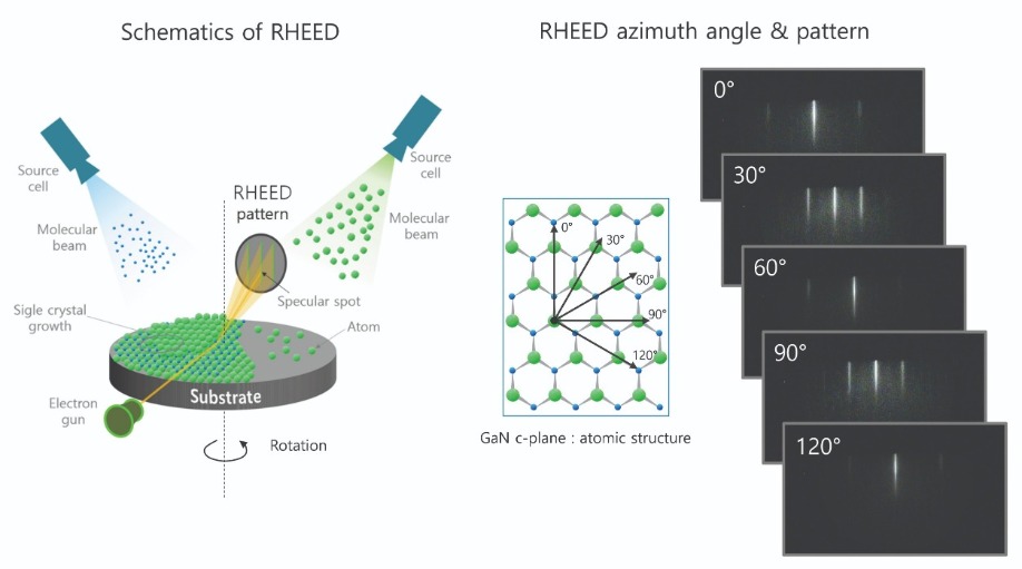
Figure 4. Real-time monitoring of the surface atomic structure during the epitaxial growth.
Recently, however, AI has moved on. Now a machine can distinguish objects in images by training, using just data itself, rather than requiring preliminary work from an engineer. The machines of today can distinguish objects in a new image by learning validity and correlation of the images on the database – they don’t need information on the actual object (see Figure 5).
This AI algorithm, called ‘deep learning’, is a major breakthrough for classifying and interpreting RHEED measurements. It allow systems to monitor, in real time, the crystal characteristics for every atomic layer in entire epistructures.
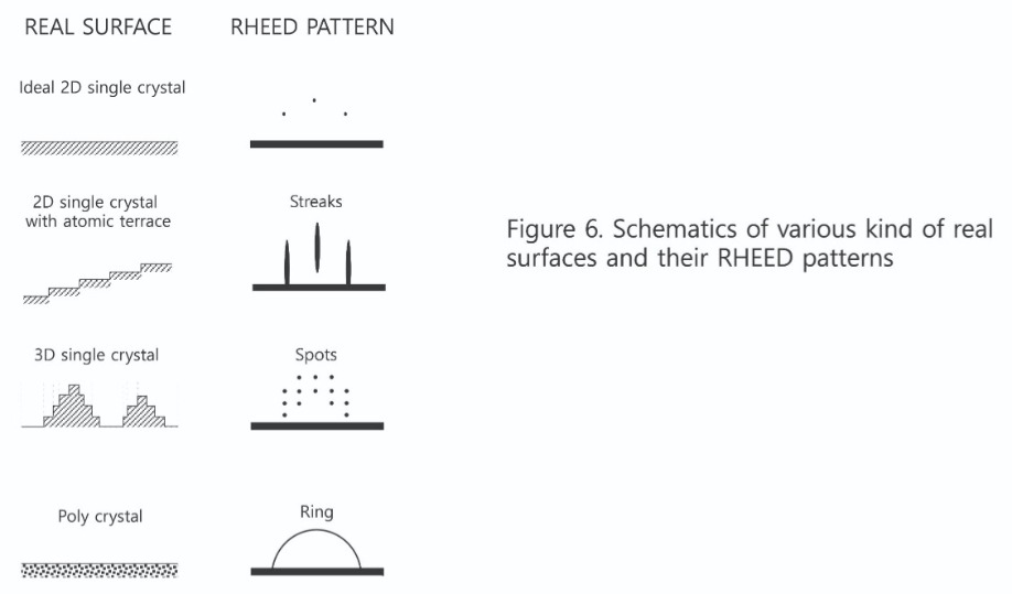
With RHEED patterns, the surface crystal structure of an epiwafer is captured by the shape of an electron diffraction pattern. For example, streaky patterns represent two-dimensional growth, those that are spotty signify three-dimensional growth, and rings reveal polycrystalline growth. Within all these patterns, there are details of crystal structure characteristics, captured in the degree, spacing, and brightness of each pattern (Figure 6).
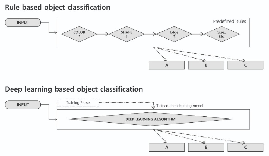
Figure 5. A comparison of conventional and deep learning methods of image classification.
When deep learning is used to recognise RHEED patterns, an inference model is created that automatically extracts high-level abstract knowledge and classifies the pattern. Features within the pattern are subjected to a multi-step feature extraction process, using the deep neural network. Quantitative modelling of RHEED patterns is difficult, because the electron diffraction patterns display various crystal growth states. However, this technology is able to automatically detect and classify various electron diffraction patterns, using inference-model, automatically learned features from the input data (see Figure 7). What’s encouraging is that the performance improves proportionally with the amount of training data, and promises to exceed that of an engineer.Using our Domm platform we can create a prediction model. It is formed by learning the validity and correlation of the dataset that integrates the classified RHEED patterns, growth conditions, and the quality results of the epiwafers. We can apply this prediction model to epiwafer manufacturing to maximise productivity (see Figure 8).
During the production of GaN-on-silicon FET epiwafers with a basic structure, our Domm system collects RHEED pattern images at up to 30 frames per second, from the beginning to the end of epiwafer growth. Commencing with thermal deoxidation on the silicon surface, and on to the growth of the AlN seed layer, the GaN buffer layer, the AlGaN barrier, and SiN passivation, our system detects and classifies the shape of the diffraction pattern for each atomic layer, along with the transition of patterns. Our model is capable of accomplishing this, thanks to training through deep learning for the entire structure. As a result, Domm monitors and intelligently analyses the manufacturing process, in addition to collecting data on growth conditions and equipment status, and determining pass/fail results.
It is challenging to determine the crystal structures of the GaN buffer layer and the GaN/AlGaN heterojunction interface. However, we are able to gain insight into this by monitoring the setting conditions – including substrate temperature, shutter sequence, and source cell temperature – and the patterns produced by the surface of the wafers, the deoxidation process, and the seed layer. What’s more, by quantitatively measuring pattern transition during the formation of the interfaces surrounding each layer, we are able to quantify the level of similarity with the manufacturing of pass products. When these results are used to predict yield in real time, or sub-standard quality, this can boost productivity, either by requesting a correction to the engineer or by automatically correcting the recipe (see Figure 9).
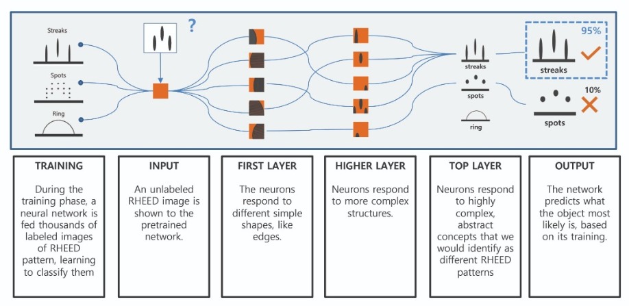
Figure 7. RHEED pattern recognition using a deep neural network.
Our efforts could help to ignite the use of AI within the compound semiconductor industry. Right now, AI is attracting more attention in the likes of: radiology, for medical diagnosis; autonomous driving for automobiles; robotics; and new drug development.As compound semiconductor manufacturing involves a number of different, complex processes that are conducted step-by-step, this hampers the construction of effective, high-quality input datasets needed for AI. But this could start to change, now that we are demonstrating that RHEED patterns can offer high-quality input data that ultimately provides the highest level of resolution for semiconductor crystal structures.
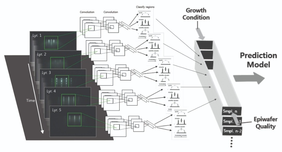
Figure 8. IVWorks patented AI epitaxy platform Domm.
However, we are in an envious position, since epiwafer production is a single-process manufacturing field. For us, the crystal growth itself becomes the product, making it a potentially optimal field for the application of AI manufacturing technology.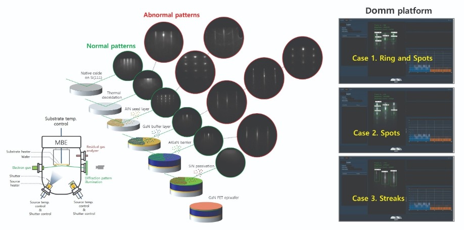
Figure 9. RHEED pattern detection and classification by Domm platform.
W. Braun, 1999. Applied RHEED : Reflection High-Energy Electron Diffraction During Crystal Growth. Springer, Berlin, NY.
A. Krizhevsky et al. 2012. Conf. Advances in Neural Information Processing Systems : ImageNet Classification with Deep Convolutional Neural Networks.
S. Hasegawa, 2012. Characterization of Materials: Reflection High-Energy Electron Diffraction. John Wiley & Sons, Inc.


