UCLA and Cardiff team deliver uncooled nanowire SWIR/MWIR detectors

Research paves the way toward integrating small bandgap photoabsorbers on large bandgap substrates
Researchers from the University of California at Los Angeles (UCLA) and Cardiff University have developed a low noise uncooled InAs(Sb) nanowire photodetection platform on InP substrate at short- and mid-wavelength infrared (SWIR/MWIR) with a two-order decrease in active material volume compared to thin films. This work paves the way toward integrating small bandgap photoabsorbers on large bandgap substrates to achieve comparable detection performance metrics to their bulk planar device counterparts.
Diana L. Huffaker, scientific director of Cardiff University's Institute for Compound Semiconductors (ICS), is leading the collaboration between UCLA and Cardiff University. She has focused her 20-year research effort on improving the performance of low-dimensional III-V compound semiconductors and optimising their applications in optoelectronic devices. This recent achievement is built upon the groups’ previous studies on III-V nanowire growth by MOCVD and their comprehensive understanding of nanowire optoelectronic device physics.
III–V semiconductor photodetectors operating in the SWIR/MWIR (1.4–5μm wavelengths) are widely used for imaging applications, such as heat seeking, night vision, remote sensing, and spectroscopy. Achieving uncooled, high-detectivity and multispectral photodetectors in these wavelength regimes is highly desirable yet challenging, as today’s photodetectors require bulky cooling technology to function at high efficiency. Devices made using current technology also possess a fundamental limit to achieving higher detectivity due to a fundamental trade-off between high responsivity and low dark current.
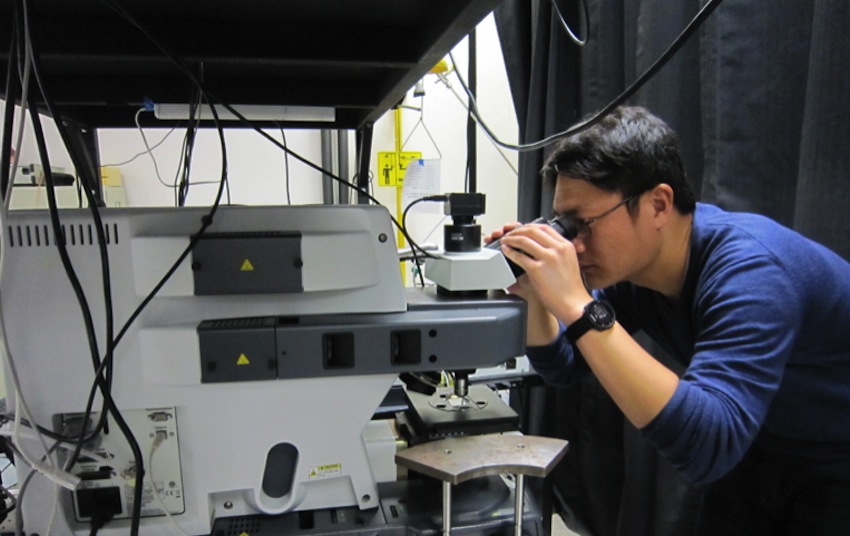
“Particularly at MWIR, high responsivity requires a thick absorption layer, which in turn results in high dark current, meaning high noise,” says Dingkun Ren (pictured above), the lead researcher at UCLA. “A new photodetection platform is thus required to boost the detectivity limit.”
To break the trade-off, Ren and the team proposed plasmonically-enhanced nanowire-based photodetection platforms composed of vertically oriented selective-area n-type InAs(Sb) nanowire photoabsorber arrays on p-type InP substrates, forming InAs−InP heterojunctions. The sum combination of the small fill factor of the nanowire arrays (reduced absorber volume) and their fabrication on large bandgap substrates decreases device dark current due to less generation-recombination and minority carrier diffusion.
The loss of the optical absorber volume is also compensated via efficient plasmonic light couplers that strongly couple and confine incident light in SWIR/MWIR to surface plasmonic modes in the nanowire top segments and are independent of the nanowire substrate optical property. “Our 3D computational photodetector model predicts a peak detectivity of 3.5e10 Jones within the wavelength regime of 2.0–3.4 μm, making it about one order higher than that of the best commercial uncooled InAs photodiodes,” says Ren. This simulation study was recently published in Nanotechnology.
The team further demonstrated two prototypes – uncooled InAs nanowire detector at SWIR with a cut-off at 2.5 µm and InAsSb nanowire detector at MWIR up to 3.4µm. The InAs(Sb) nanowire arrays were grown by selective-area MOCVD with extremely high vertical yield and high uniformity. “This heteroepitaxy is achieved by elastically accommodating the lattice mismatch strain through nanowire sidewall facets, a prospect infeasible in thin-film epitaxy,” Ren comments.
The team further developed a passivation technique based on aluminum oxide to largely suppress surface recombination on InAsSb nanowire surfaces. Those two prototypes showed room-temperature photodetection with suppressed noise and plasmonically-enhanced detection peaks, the first demonstration of nanowire-based SWIR and MWIR uncooled photodetectors.
“Note that the unique plasmonic structure in our devices opens the possibility of developing nanowire-plasmonic multichannel detectors for multispectral and hyperspectral imaging applications,” says Khalifa Azizur-Rahman, the lead researcher from the Cardiff lab. Those two prototypes were recently reported in two papers in Nano Letters, and the work for MWIR was featured as a Supplementary Cover Article.
“We demonstrated the feasibility of achieving high detectivity at room-temperature at SWIR/MWIR by using InAs(Sb)-InP nanowire-plasmonic heterojunction photodiodes,” says Ren. “Indeed, there are many challenges ahead to commercialize such nanowire devices and compete with their bulk counterparts. One demanding factor is the wafer-scale epitaxy capability of InAs(Sb) nanowire arrays on 6-inch InP substrates. And this certainly requires a large amount of research efforts. Additionally, there is still room to improve the plasmonic structures and nanowire passivation.”
The team’s work provides a foundation for achieving room-temperature operation of nanowire photodetectors at SWIR/MWIR or even longer wavelengths with significant applications in both industrial and research settings. “We are very excited about what we have achieved so far. We are also looking for more collaborations to carry on this research,” says Khalifa.
'Room-temperature mid-wavelength infrared InAsSb nanowire photodetector arrays with Al2O3 passivation' by D. Ren et al; Nano Letters, 19, 2793-2802, 2019. (Supplementary Cover Article)
'Uncooled photodetector at short-wavelength infrared using InAs nanowire photoabsorbers on InP with p-n heterojunctions' by D. Ren et al; Nano Letters, 18, 7901–7908, 2018.
'Feasibility of achieving high detectivity at short-and mid-wavelength infrared using nanowire-plasmonic photodetectors with p-n heterojunctions' by D. Ren et al; Nanotechnology, 30, 044002, 2018.


