
Researchers show 6.1eV direct bandgap for monolayer BN
Hexagonal BN could be a promising optoelectronic material with highly efficient emission in deep ultraviolet
High-temperature MBE offers new opportunities in the burgeoning field of 2D materials and related van der Waals heterostructures. Now scientists at Nottingham University (UK) and Montpellier University (France) have applied this technology to hexagonal boron nitride (hBN).
Whereas bulk hBN is an indirect band-gap material, theoretical work has predicted that hBN becomes direct gap in the atomic monolayer limit.
MBE growth and atomic-force microscopy at Nottingham University were complemented by reflectance and photoluminescence spectroscopy at Montpellier University, revealing a direct band-gap at 6.1 eV (wavelength 205 nm) for monolayer thick boron nitride.
The demonstration of a direct band-gap in monolayer hBN grown by the scalable approach of MBE makes it a promising optoelectronic material with highly efficient emission in the deep ultraviolet (DUV).
Monolayer boron nitride was synthesised before the discovery of graphene by decomposing of borazine on a metal surface. It was later produced by exfoliation or electron beam thinning of bulk crystals of hBN. Recently, wafer-scale single-crystals of monolayer boron nitride were reported by chemical vapour deposition. For these fabrication methods, luminescence could only be detected down to 6 monolayers, leaving unanswered the question of emission from monolayer hBN.
The Montpellier – Nottingham team have resolved this issue using a strategy which relies on the scalable growth of monolayer boron nitride and which enables macroscopic photoluminescence and reflectance measurements. Their wafer-scale layers are grown by high-temperature MBE on highly oriented pyrolytic graphite substrates.
The closely lattice-matched graphite substrate enables synthesises of monolayer boron nitride by van der Waals epitaxy with an interface free from intermixing effects. With reflectance measurements on monolayer hBN showing a pronounced resonance at around 6.1 eV, photoluminescence experiments now reveal emission at this energy.
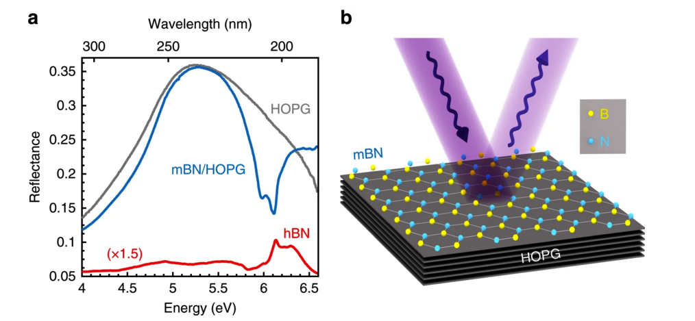
The picture at the top shows the reflectance of epitaxial monolayer BN on graphite. a) Reflectance spectrum in the deep ultraviolet for the bare graphite substrate (grey line), mBN on graphite (blue line), and bulk hBN (red line), at 10 K. b Schematic of the reflectance experiment performed on the mBN-graphite heterostructure synthesised by van der Waals epitaxy. HOPG stands for highly oriented pyrolytic graphite
The absence of a Stokes-shift between reflectance and photoluminescence contrasts with multilayer and bulk hexagonal boron nitride, thus providing the signature of a direct-gap in monolayer boron nitride.
The researchers intend to further develop the growth of hBN for deep ultraviolet (DUV) applications, perform graphene encapsulation and graphene/hBN superlattices.
'Direct band-gap crossover in epitaxial monolayer boron nitride' by, C. Elias et al; Nature Communications 10, 2639 (2019).


