
Aixtron targets 2D technology
Wafers featuring 2D layered materials and sandwich heterostructures "are just around the corner"
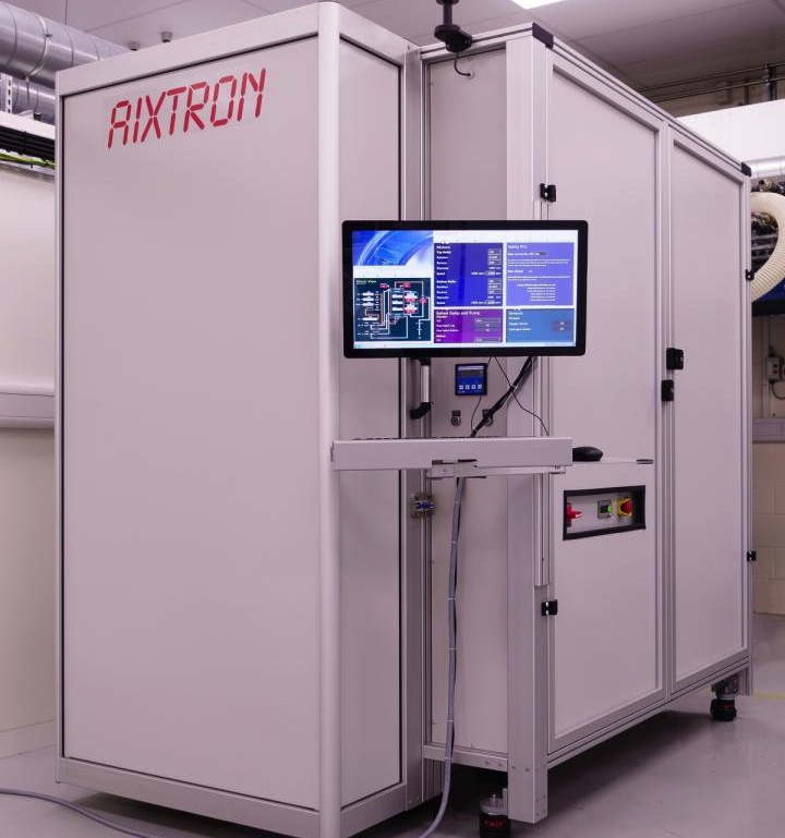
Graphene Flagship partner Aixtron has demonstrated two new systems - the Neutron and the CCS 2D reactor - that enable the large-scale production of graphene and other 2D layered materials through chemical vapour deposition.
Kari Hjelt, Head of Innovation of the Graphene Flagship said "these discoveries open up thousands of possibilities beyond graphene, the arrival of wafers featuring other layered materials, or even 'sandwich' heterostructures are just around the corner," concludes Hjelt.
The Neutron is a roll-to-roll system capable of depositing large areas of graphene on metal foils under ambient conditions. The CCS 2D system enables wafer-scale production of graphene on insulating wafers and is also capable of large-scale production of other layered materials, such as boron nitride or transition metal dichalcogenides.
During the first years of the Graphene Flagship project, together with the group of Camilla Coletti at Graphene Flagship partner Istituto Italiano di Tecnologia (IIT), Aixtron scaled the growth of graphene on insulators to full wafer-scale on its CCS 2D reactor, which can accommodate 2-inch up to 8-inch wafers. The wafers exhibit low contamination levels that meet the requirements of semiconductor fabs directly after growth. Camilla Coletti comments that "such tremendous progress is only possible thanks to the Graphene Flagship project which brings together top scientists from academia and engineers from a world-leading equipment company."
Andrea C. Ferrari, Science and Technology Officer of the Graphene Flagship and Chair of its Management Panel added that "the ultimate aim of the Graphene Flagship is to bring graphene and related layered materials from the lab to the factory floor. To take these new materials to the traditional semiconductor fabs, which is key to achieve their widespread application in consumer electronics, photonics and sensors, industrial tools capable of large area, large rate and low-cost manufacturing of graphene and related materials are needed."


