
Atomic 'patchwork' for next gen semiconductor devices
Japanese researchers show continuous process for engineering 2D transition metal dichalcogenide heterostructures
Researchers from Tokyo Metropolitan University have grown atomically thin crystalline layers of transition metal dichalcogenides (TMDCs) with varying composition over space, continuously feeding in different types of TMDC to a growth chamber to tailor changes in properties.
Examples include 20nm strips surrounded by different TMDCs with atomically straight interfaces, and layered structures. They also directly probed the electronic properties of these heterostructures; potential applications include electronics with unparalleled power efficiency.
A broad range of scientific research has been directed to the next steps in semiconductor design, particularly the application of novel materials to engineer more compact, efficient circuitry which leverages the quantum mechanical behaviour of materials at the nanometer length scale. Of special interest are materials with a fundamentally different dimensionality; the most famous example is graphene, a 2D lattice of carbon atoms which is atomically thin.
TMDCs are promising candidates for incorporation into new semiconductor devices. Composed of transition metals like molybdenum and tungsten and a chalcogen (or Group 16 element) like sulphur or selenium, they can form layered crystalline structures whose properties change drastically when the metallic element is changed, from normal metals to semiconductors, even to superconductors.
By controllably weaving domains of different TMDCs into a single heterostructure (made of domains with different composition), it may be possible to produce atomically thin electronics with distinct, superior properties to existing devices.
A team led by Yu Kobayashi and Yasumitsu Miyata from Tokyo Metropolitan University has been at the cutting edge of efforts to create 2D heterostructures with different TMDCs using vapour-phase deposition, the deposition of precursor material in a vapour state onto a surface to make atomically flat crystalline layers.
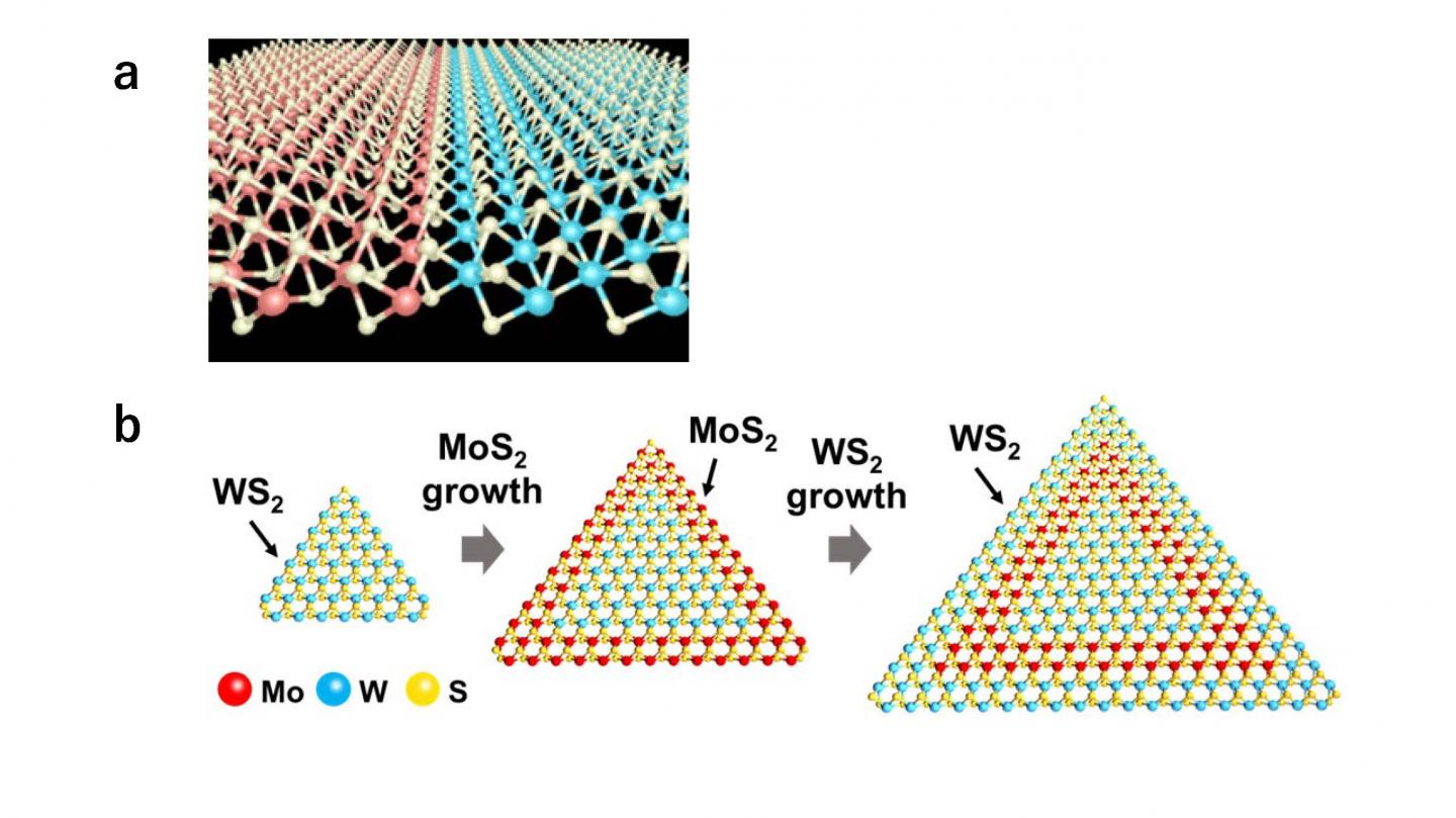
Pictured at the top of the page: (a) Red and blue are different metal atoms; yellow are chalcogen atoms. (b) Newly developed procedure. Different TMDC precursors are fed in sequentially to grow crystalline domains with different composition.
One of the biggest challenges they faced was creating a perfectly flat interface between different domains, an essential feature for getting the most out of these devices. Now, they have succeeded in engineering a continuous process to grow well-defined crystalline strips of different TMDCs at the edge of existing domains, creating strips as thin as 20nm with a different composition.
Their new process uses liquid precursors which can be sequentially fed into a growth chamber; by optimising the growth rate, they were able to grow heterostructures with distinct domains linked perfectly over atomically straight edges.
They directly imaged the linkage using scanning tunnelling microscopy (STM), finding excellent agreement with first-principles numerical simulations of what an ideal interface should look like. The team used four different TMDCs, and also realised a layer-on-layer heterostructure.
By creating atomically sharp interfaces, electrons may be effectively confined to one-dimensional spaces on these 2D devices, for exquisite control of electron transport and resistivity as well as optical properties. The team hopes that this may pave the way to devices with unparalleled energy efficiency and novel optical properties.
'Continuous Heteroepitaxy of Two-Dimensional Heterostructures Based on Layered Chalcogenides' by Yu Kobayashi et al; ACS Nano May 31, 2019


