Loading...
News Article

Swiss team discovers spontaneous CdSe nanotubes

News

Automatically assembling tubes have between three and six walls that are perfectly uniform and just a few atoms thick

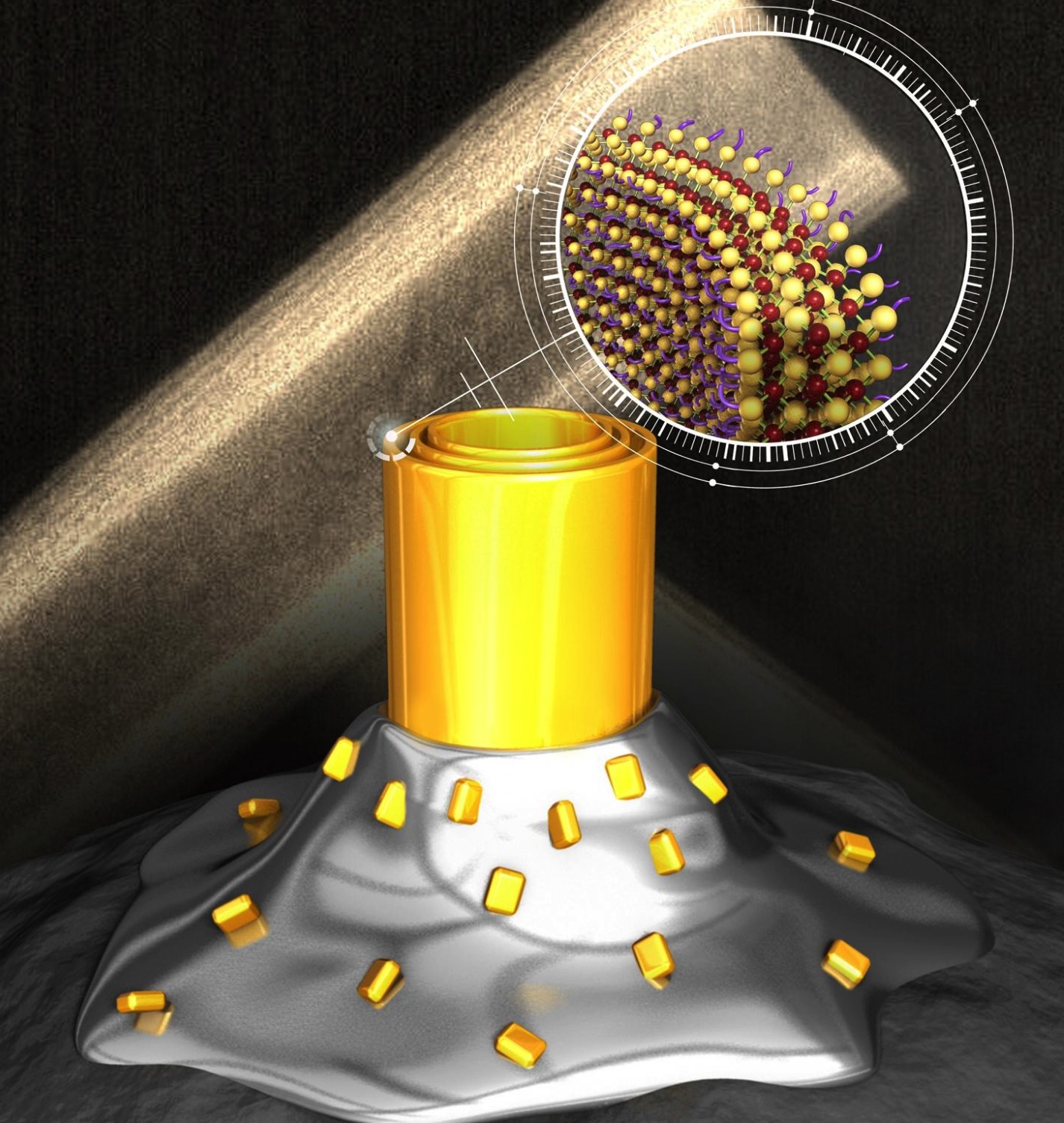
Researchers at the Ecole Polytechnique Federale de Lausanne (EPFL) in Switzerland have discovered semiconducting nanotubes made of CdSe that assemble automatically in solutions of metallic nanocrystals and certain ligands. The tubes have between three and six walls that are perfectly uniform and just a few atoms thick - making them the first such nanostructures of their kind.

What's more, the nanotubes possess photoluminescent properties: they can absorb light of a specific wavelength and then send out intense light waves of a different colour, much like quantum dots and quantum wells.

That means they can be used as fluorescent markers in medical research, for example, or as catalysts in photoreduction reactions, as evidenced by the removal of the colours of some organic dyes, based on the results of initial experiments. The researchers' findings have made the cover of ACS Central Science.

An accidental discovery

But the unique feature of these semiconducting nanotubes is how they are formed. "Our discovery happened almost by chance. We had set out to study the role that certain ligands play in making 2D semiconducting nanometric crystals," says Xiaopeng Huang, the study's lead author. But the research team found that some ligands caused molecules to spontaneously come together in precise cylindrical structures which until then had been impossible to create.

The researchers will now investigate the other physical and electrical properties of their nanotubes and look into methods for making nanotubes with just a single wall.

'Spontaneous Formation of CdSe Photoluminescent Nanotubes with Visible-light Photocatalytic Performance' by Xiaopeng Huang et al; ACS Central Science. 2019, 5, 6, 1017-1023

SiC MOSFETs: Understanding the benefits of plasma nitridation
Wolfspeed reports Q2 results
VueReal secures $40.5m to scale MicroSolid printing
Mitsubishi joins Horizon Europe's FLAGCHIP project
Vishay launches new high voltage SiC diodes
UK team leads diamond-FET breakthrough
GaN adoption at tipping point, says Infineon
BluGlass files tuneable GaN laser patents
QD company Quantum Science expands into new facility
Innoscience files lawsuit against Infineon
Riber revenues up 5% to €41.2m
Forvia Hella to use CoolSiC for next generation charging
Photon Design to exhibit QD simulation tool
Ortel transfers CW laser fabrication to Canada
Luminus adds red and blue multi-mode Lasers
PseudolithIC raises $6M for heterogeneous chiplet tech
Mesa sidewall design improves HV DUV LEDs
IQE revenue to exceed expectations
'Game-changing' VCSEL system targets clinical imaging
German start-up secures finance for SiC processing tech
Macom signs preliminaries for CHIPS Act funding
IQE and Quintessent partner on QD lasers for AI
EU funds perovskite tandems for fuel-free space propulsion
EU to invest €3m in GeSi quantum project
Transforming the current density of AlN Schottky barrier diodes
Turbocharging the GaN MOSFET with a HfOâ‚‚ gate
Wolfspeed launches Gen 4 SiC MOSFET technology
Report predicts high growth for UK's North East
Element Six unveils Cu-diamond composite
SemiQ launches hi-rel 1700V SiC MOSFETs
Lynred to exhibit Eyesential SWIR sensor for machine vision
Thorlabs buys VCSEL firm Praevium Research
×
Search the news archive

To close this popup you can press escape or click the close icon.
Logo
x
Logo
×
Register - Step 1

You may choose to subscribe to the Compound Semiconductor Magazine, the Compound Semiconductor Newsletter, or both. You may also request additional information if required, before submitting your application.


Please subscribe me to:


You chose the industry type of "Other"

Please enter the industry that you work in: