
Nanoscale visualisation of dopant in GaN
Significant advances in the understanding of P-Type GaN semiconductor formation mechanisms and techniques enabling mass production of GaN devices
Scientists at the National Institute for Materials Science (NIMS) in Japan have succeeded for the first time in visualising at the nanoscale the distribution and optical behaviour of GaN implanted with a small amount of magnesium. They believe this may help in improving electrical performance of GaN based devices.
They have also revealed some of the mechanisms by which introduced magnesium ions convert GaN into a p-type semiconductor. These findings may significantly expedite the identification of optimum conditions for magnesium implantation vital to the mass production of GaN power devices.
The development of GaN based power devices requires fabrication of both n- and p-type GaN semiconductors. p-type GaN semiconductors can be mass produced by introducing magnesium ions into GaN wafers and subjecting the wafers to thermal treatment.
However, no method existed for assessing the effect of magnesium concentrations and thermal treatment temperature on the distribution and optical behaviour of magnesium implanted into GaN at nanoscale dimensions. In addition, the mechanisms by which p-type GaN forms remained unclear so far. These issues had been hindering the development of technologies enabling mass production of GaN devices.
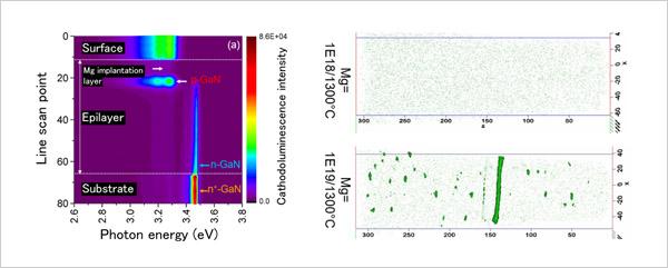
For this research, the team prepared slanted cross-sections of magnesium ion-implanted GaN wafers by polishing the wafers at an angle and analysed the distribution of luminescence intensity on the cross-sections using a cathodoluminescence technique. As a result, they found that magnesium atoms implanted several tens of nanometers beneath the wafer surface had been activated while those immediately below the surface had not been activated (figure at left).
In addition, they found using atom probe tomography that magnesium atoms, when implanted in high concentrations, develop into either disc- or rod-shaped deposits depending on temperature (figure at right).
The integration of different analytical results generated by these latest microscopy techniques indicated that magnesium atoms implanted in the vicinity of the wafer surface may develop into deposits under certain temperature conditions, and thus prevents them from activating.
The results of this research have provided vital guidance for the development of ion-doped p-type GaN layers. Furthermore, the techniques developed during this project for the analysis of impurity distributions are applicable not only in homogeneous wafers but also in GaN device materials with varying structures. The use of these techniques may therefore speed the development of high-performance GaN devices.
Part of this research was published online in Applied Physics Express, a journal of the Japan Society of Applied Physics, on April 11, 2019.


