
Bluglass awarded Key US Tunnel Junction Patent
Buried activated p-(Al,In)GaN layer technology has potential in high-brightness LEDs, micro-LEDs, laser diodes, solar cells, and other optoelectronic and power electronics devices
Australian semiconductor company BluGlass has announced that the United States Patent and Trademark Office has issued US Patent 10,355,165, Buried Activated p-(Al,In)GaN Layers. This proprietary technology has significant performance potential in a number of applications including high-brightness LEDs, micro-LEDs, laser diodes, solar cells, and other optoelectronic and power electronics devices.
BluGlass’ RPCVD-grown buried activated p-GaN layers can help address one of the LED industry’s critical challenges: “efficiency droop”. The efficiency of an LED is a measure of how much light output is generated for a given amount of electrical power used to drive the device. Efficiency droop is where the efficiency of an LED reduces as operating power is increased. This challenge results in many of today’s high-powered LEDs being operated outside their peak efficiency.
Incremental efficiency improvements continue to be a major objective for LED manufacturers.
One potential resolution of efficiency droop is multi-junction or cascade devices (LEDs or laser diodes as examples). RPCVD’s buried activated p-GaN layers are a critical building block to enable the tunnel junction, which in turn allows multiple LEDs to be grown in a continuous vertical stack and interconnected in a single, high efficiency chip, called a cascade LED. As a result, less power is needed to deliver the desired light output, potentially eliminating efficiency droop
and significantly increasing device performance.
Cascade LEDs are expected to enable smaller, cheaper and higher performing LEDs – the three key interest areas of the LED industry. To date, functioning tunnel junctions, and therefore cascade LEDs, have been prohibitively difficult to produce due to the challenges in achieving buried activated p-GaN using conventional growth technologies such as MOCVD.
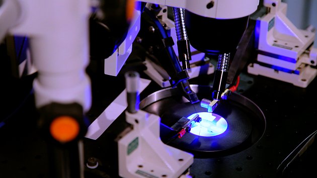
BluGlass is developing and commercialising a unique Australian technology called remote plasma chemical vapour deposition (RPCVD), a revolutionary approach to the manufacture of group III nitrides which are essential components used in millions of electronics devices globally. RPCVD offers better-performing, lower-cost devices and more environmentally sustainable processes for electronics manufacturers producing LEDs for automotive and overhead lighting, microLEDs for wearables and virtual reality display and power electronics for efficient power conversion.
BluGlass’ Managing Director, Giles Bourne said “This patent adds an important cornerstone to BluGlass’ intellectual property portfolio, protecting our unique RPCVD process, hardware and competitive advantages. RPCVD allows us to develop this elegant new option for resolving the challenges of efficiency droop in high-performance LEDs - something that's been very difficult to resolve using the industry standard MOCVD technology.” “Our growing strategic patent portfolio, comprising 63 internationally granted patents, continues to underpin the commercialisation of our RPCVD technology across a range of market segments with long-term market exclusivity”. BluGlass has received strong interest on the performance potential of RPCVD tunnel junctions and cascade LEDs from
the industry. Discussions with a number of groups are continuing.


