
UCLA team shows SAM-APDs for Gamma-ray detection
Proof-of-concept antimonide-based detectors show well-defined X-ray and Gamma-ray response spectra
Researchers from UCLA have demonstrated the first antimonide-semiconductor-based (Sb-based) separate absorption and multiplication avalanche photodiodes (SAM-APDs) capable of mapping the energy spectra of X-ray and Gamma-ray photons.
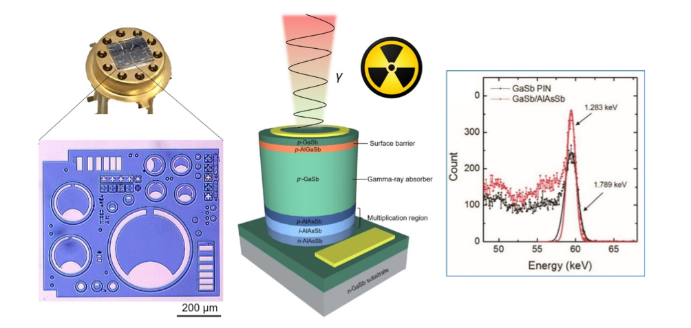
In their recent paper in Adv. Optical Mater, the team has shown how combining two semiconductor compound materials, GaSb and AlAsSb, enhances the probability of 'absorbing' high energy photons while drastically suppressing the device noise. The paper also shows well-defined X-ray and gamma-ray photopeaks under 241Am radioactive sources up to 59.5 keV with a full-width half-maximum of 1.283 keV.
To capture gamma-rays and understand their interaction with matters, it is critical to use high-performance energy-sensitive detectors. Different from regular detectors for visible light or infrared, those energy-sensitive detectors need to sustain incident radiations with extremely high energy over 100 keV (considering a photon of green light which is only about 2 eV).
The research team consists of experts in epitaxial growth at the California NanoSystems Institute, fabrication of III-V semiconductor devices at the Department of Electrical and Computer Engineering, and gamma-ray detection at the Department of Molecular and Medical Pharmacology. It is led by Diana Huffaker, Arion Chatziioannou, and Baolai Liang.
The capability of resolving energies in X-ray and gamma-ray spectra is mainly determined by the choice of detector material. Si, Ge and GaAs are the work-horses in the radiation detection industry but GaSb is more promising. “GaSb wins because it shows much better absorption efficiency to high-energy radiations than Si and Ge. Additionally, it can provide a much higher probability than GaAs to stop X-ray and gamma-ray photons due to its relatively higher atomic number,” said Bor-Chau Juang, lead researcher.
Dingkun Ren, a device and material expert, comments: “People have been developed different types of SAM-APDs for decades. However, there have been no reported SAM-APDs for high-energy radiations. We made the first ones. The SAM structure can offer much higher signal-to-noise ratio due to its internal gain from large bandgap multiplication region. We chose AlAsSb for the multiplication region due to its lattice-match with the absorber material GaSb.”
“Additionally, the GaSb/AlAsSb material system provides a larger dissimilarity in both pair creation energy and absorption efficiency. Thus, it adds an additional merit to reduce any spurious photopeaks outside the GaSb absorption regions,” says Ren.
The detectors were grown by MBE and tested with a 0.74 MBq 241Am radioactive source. The measurements show a distinct peak at 59.5 keV with an FWHM of 1.283±0.082 keV. In addition, they observed more signature energy lines, which are well-defined, such as Ga-Kα escape peak at 50.3 keV, Sb-Kα escape peak at 33.2 keV and more. “We note our SAM-APDs show much narrower photopeak at 59.5 keV than our previous GaSb photodiodes. This clearly indicates the SAM structure help eliminating spurious signals due to large differences in pair creation energy and absorption efficiency between GaSb and AlAsSb,” said Juang.
This technology can be used to detect radiations with even higher energies. Liang adds, “Our work paves the way to achieving efficient detection of high-energy radiations in various applications. We welcome more collaborations to carry on this research.”
The research was supported by the Defense Threat Reduction Agency (DTRA) and National Science Foundation (NSF) of the United States.
'Energy-Sensitive GaSb/AlAsSb Separate Absorption and Multiplication Avalanche Photodiodes for X-Ray and Gamma-Ray Detection' by Bor-Chau Juang et al; Adv. Optical Mater. 7, 1900107 (2019)


