
First-ever visualisations of electrical gating effects
Technique gives new insight into bandgaps of 2D semiconductors, say researchers
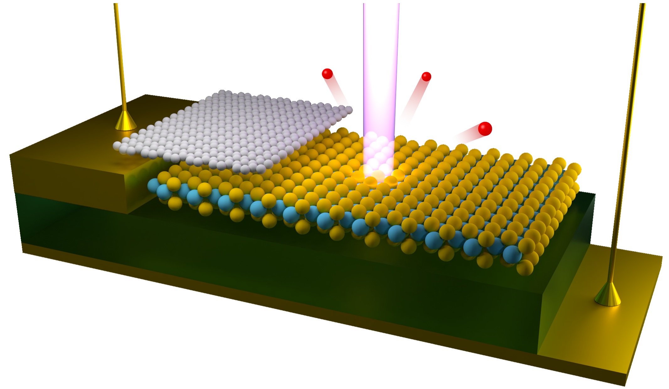
Physicists from the University of Warwick and the University of Washington have developed a technique to measure the energy and momentum of electrons in operating microelectronic devices made of atomically thin, 2D materials. They first tested the technique using graphene before applying it to 2D transition metal dichalcogenide (TMD) compound semiconductors.
Using this information, they say they can create visual representations of the electrical and optical properties of the materials to guide engineers in maximising their potential in electronic components. The study ‘Visualising electrostatic gating effects in two-dimensional heterostructures’ was published in Nature (17 July.
By applying this technique scientists will have the information they need to develop ‘fine-tuned’ electronic components that work more efficiently and operate at high performance with lower power consumption. It will also help in the development of 2D semiconductors that are seen as potential components for the next generation of electronics, with applications in flexible electronics, photovoltaics, and spintronics.
Neil Wilson from the University of Warwick’s Department of Physics said: “ This work is at the fundamental level and is a big step in understanding materials and the science behind them. The new insight into the materials has helped us to understand the band gaps of these semiconductors, which is the most important parameter that affects their behaviour, from what wavelength of light they emit, to how they switch current in a transistor.”
The technique uses angle resolved photoemission spectroscopy (ARPES) to ‘excite’ electrons in the chosen material. By focusing a beam of ultra-violet or x-ray light on atoms in a localised area, the excited electrons are knocked out of their atoms. Scientists can then measure the energy and direction of travel of the electrons, from which they can work out the energy and momentum they had within the material (using the laws of the conservation of energy and momentum). That determines the electronic structure of the material, which can then be compared against theoretical predictions based on state-of-the-art electronic structure calculations performed in this case by the research group of co-author Nicholas Hine.
The measurements were taken at the Spectromicroscopy beamline at the ELETTRA synchrotron in Italy, in collaboration with Alexei Barinov and his group there.
David Cobden, professor in the Department of Physics at the University of Washington, said: “It used to be that the only way to learn about what the electrons are doing in an operating semiconductor device was to compare its current-voltage characteristics with complicated models. Now, thanks to recent advances which allow the ARPES technique to be applied to tiny spots, combined with the advent of 2D materials where the electronic action can be right on the very surface, we can directly measure the electronic spectrum in detail and see how it changes in real time. This changes the game.”
Xiaodong Xu, from the Department of Physics and the Department of Materials Science and Engineering at the University of Washington, said: “This powerful spectroscopy technique will open new opportunities to study fundamental phenomena, such as visualisation of electrically tuneable topological phase transition and doping effects on correlated electronic phases, which are otherwise challenging.”
The research was supported by the Engineering and Physical Sciences Research Council, part of UK Research and Innovation, and the US Department of Energy and the National Science Foundation.


