
2D perovskite materials found to have conductive edges
Metal-like properties could provide new way to improve performance of next-generation optoelectronics and nanogenerators
Researchers at Penn State University in the USA have discovered a new class of 2D perovskite materials with edges that are conductive like metals and cores that are insulating.
"This observation of the metal-like conductive states at the layer edges of these 2D perovskite materials provides a new way to improve the performance of next-generation optoelectronics and develop innovative nanoelectronics," said Kai Wang, assistant research professor in materials science and engineering at Penn State and lead author on the study.
Wang and a team of Penn State researchers made the discovery while synthesising lead halide perovskite materials for use in next generation solar cells.
The findings, reported in Science Advances, provide new insights into the charge and energy flow in perovskite materials, important for the continued advancement of the technology, the scientists said.
"I think the beauty of this work is that we found a material that has completely different properties along the edges compared to the core," said Shashank Priya, professor of materials science and engineering and associate vice president for research at Penn State. "It's very unusual that the current can flow around the edges and not in the center of a material, and this has huge implications for the design of solar cell architectures."
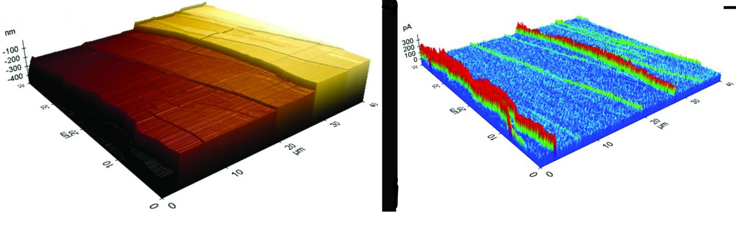
The 2D perovskite materials they studied consist of thin, alternately stacked organic and inorganic layers. The organic layers protect the inorganic layers of lead halide crystals from moisture that can degrade 3D versions of the material. This layered structure results in a large variation in conductivity along perpendicular and parallel directions. The picture above shows topographical views of the surface of the perovskite layer and electrical current image of the same layer show conductive edges
Using scanning and mapping techniques, the researchers found that sharp edges of the 2D single crystals exhibited extraordinarily large free charge carrier density. "This work reveals the distinct differences in optoelectronic properties between the crystal layer edge and the core region, which can give a hint toward answering other important questions raised in the field of optoelectronics about these 2D perovskite materials," Wang said.
Researchers said the findings could boost performance of solar cells and LED technology by providing additional charge pathways within the devices. The findings also open the door for the development of innovative one-dimensional electrical conduction in nanoelectronics.
"Across the length of these materials, you have a junction between metal and semiconductor, and there are a lot of hypothetical devices proposed based on that junction," Priya said.
Because of the strong current found at the edges, 2D perovskite crystals may also be a good candidate for a triboelectric nanogenerator, the researchers said. Nanogenerators convert motion into electric power, which could lead to wearable technology that charges phones and other devices using both light and mechanical energy and inputs.
'Distinct conducting layer edge states in two-dimensional (2D) halide perovskite' by Kai Wang et al; Science Advances 12 Jul 2019


