
Improving efficiency and brightness of perovskite LEDs
Research team developed a new technique to improve the performance of organic LEDs for combined electronics and light applications
Improving efficiency, brightness of perovskite LEDs
A research team developed a new technique to improve the performance of organic LEDs for combined electronics and light applications
A recent study, published in Applied Physics Reviews explores a new approach to optimising highly efficient perovskite LEDs using an exciton confinement effect.
To achieve an efficient electroluminescent device, it must have a high photoluminescence quantum yield emission layer, efficient electron hole injection and transport layers, and high light out-coupling efficiency.
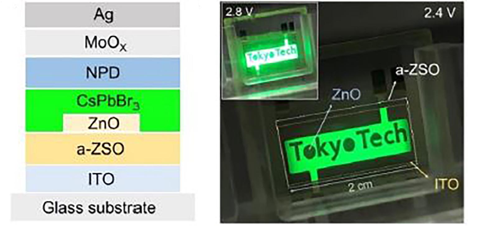
To accomplish this goal, the authors of the study explored the performance of an amorphous zinc-silica-oxide system layered with perovskite crystals to improve the diode performance.
"We think that many people [are] too focused on an emission layer," said Hideo Hosono, corresponding author on the study. "For a device, all layers are equally important since each layer has a different [but] crucial role."
The amorphous zinc silicon oxide has a shallow tuneable electron affinity, capable of confining excitons, but also high electron mobility to transport electrons. By layering the perovskite crystal and the amorphous zinc silicon oxide, the team developed a way to confine excitons and inject the electrons into the 3D perovskite layers efficiently. The energy-level alignment between the layers proved an ideal material for this purpose.
To validate their findings, the team tested their creation by producing blue, red and green perovskite LEDs, called PeLEDs. The green diode operated at the lowest voltage (2.9 volts at 10,000 candela per square meter) and was the most efficient (33 lumens/watt) and brightest (500,000 candela per square meter). While the team produced the maximum luminance for red diodes to date, the illumination remained too dim for practical use.
The image above shows the structure a large perovskite LED, where a layer of zinc oxide was deposited on the a-zinc silicate electron transport layer, providing greater brightness with better power efficiency.
While these results show the promise of manipulating the electron transport layer material, challenges remain, including the stability of perovskite materials and toxicity of lead in the mineral crystal matrix. Despite these limitations, the results offer new opportunities to apply this approach to realize practical applications for perovskite LEDs in optoelectronic devices.
"For practical PeLEDs, new halide emitting materials with chemically stability and lead-free elements are highly needed," said Junghwan Kim, corresponding author on the study. "If this issue is solved, the PeLEDs would be commercialised for practical electronics in the future."
'Performance boosting strategy for perovskite light-emitting diodes' by Kihyung Sim; Applied Physics Reviews on July 30, 2019


