
Another way to boost Halide perovskite performance?
Reducing dislocation densities leads to a four times increase in electron lifetime
A group of researchers at Rensselaer Polytechnic Institute, in the USA, and other universities, has shown that a specific defect impacts the ability of halide perovskite to hold energy derived from light in the form of electrons. The results are published in Nature Communications.
"Defects could be good or bad in semiconductors," said Jian Shi, associate professor of materials science engineering. "For some reason, people did not pay attention to dislocations in halide perovskite, but we have shown that this defect is a problem in halide perovskite."
Research on halide perovskite has rapidly improved the efficiency of the material from about a 3 percent conversion of light to electrical energy to 25 percent - equivalent to state-of-the-art silicon solar cells - over the course of a decade. Researchers wrestled with silicon for decades to reach that material's current level of efficiency.
Halide perovskite also has promising carrier dynamics, which are roughly defined as the length of time that light energy absorbed by the material is retained in the form of an excited electron. To make a good prospect for solar energy conversion, electrons in the material must retain their energy long enough to be harvested by an electrode attached to the material, thus completing the conversion of light to electrical energy.
The material had long been considered 'defect tolerant' meaning flaws like missing atoms, shoddy bonds across grains of the crystal, and a mismatch known as crystallographic dislocation were not believed to have much impact on efficiency. More recent research has questioned that assumption and found that some defects do affect aspects of the crystal's performance.
Shi's team tested whether the defect of crystallographic dislocation impacts carrier dynamics by growing the crystal on two different substrates. One substrate had a strong interaction with the halide perovskite as it was being deposited, producing a higher density of dislocations. The other had a weaker interaction and produced a lower density of dislocations.
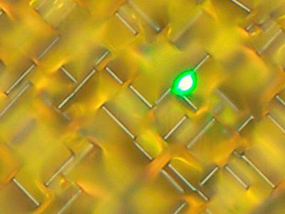
The results show that dislocations negatively impact the carrier dynamics of halide perovskite. Reducing dislocation densities by more than one order of magnitude is found to lead to an increase of electron lifetime by four times. (The electron's lifetime can be evaluated from analysing the green illuminating spot on perovskite crystals featured by the perpendicular ridges as shown the picture above).
"A conclusion is that halide perovskite has a similar dislocation effect as conventional semiconductors," Shi said. "We need to be careful of dislocations in halide perovskite, which is a factor people have been ignoring as they work on this material."
Shi's last significant work on halide perovskite revealed the role of pressure on this semiconductor's optical properties published in Science Advances in 2018.
Shi was joined by researchers from the Kunming University of Science and Technology, Tsinghua University, University of Science and Technology Beijing, Forschungszentrum Julich, and Brown University.
'Carrier lifetime enhancement in halide perovskite via remote epitaxy' by Jie Jiang et al; Nature Communications, volume 10, Article number: 4145 (2019)


