
Integration boosts deep UV LED efficiency
Monolithic integration of deep UV LED with a multiplicative photoelectric converter achieves a record high wall plug efficiency of 21.6 percent
Scientists have reported the first monolithic integration of a deep ultraviolet LED with a multiplicative photoelectric converter. The device, reported in Nano Energy, achieves a record high wall plug efficiency of 21.6 percent.
The research 'Monolithic integration of deep ultraviolet LED with a multiplicative photoelectric converter' was carried out by Changqing Chen, Yihua Gao and Jiangnan Dai from Huazhong University of Science and Technology, Zi-Hui Zhang from Hebei University of Technology and Haiding Sun from University of Science and Technology of China.
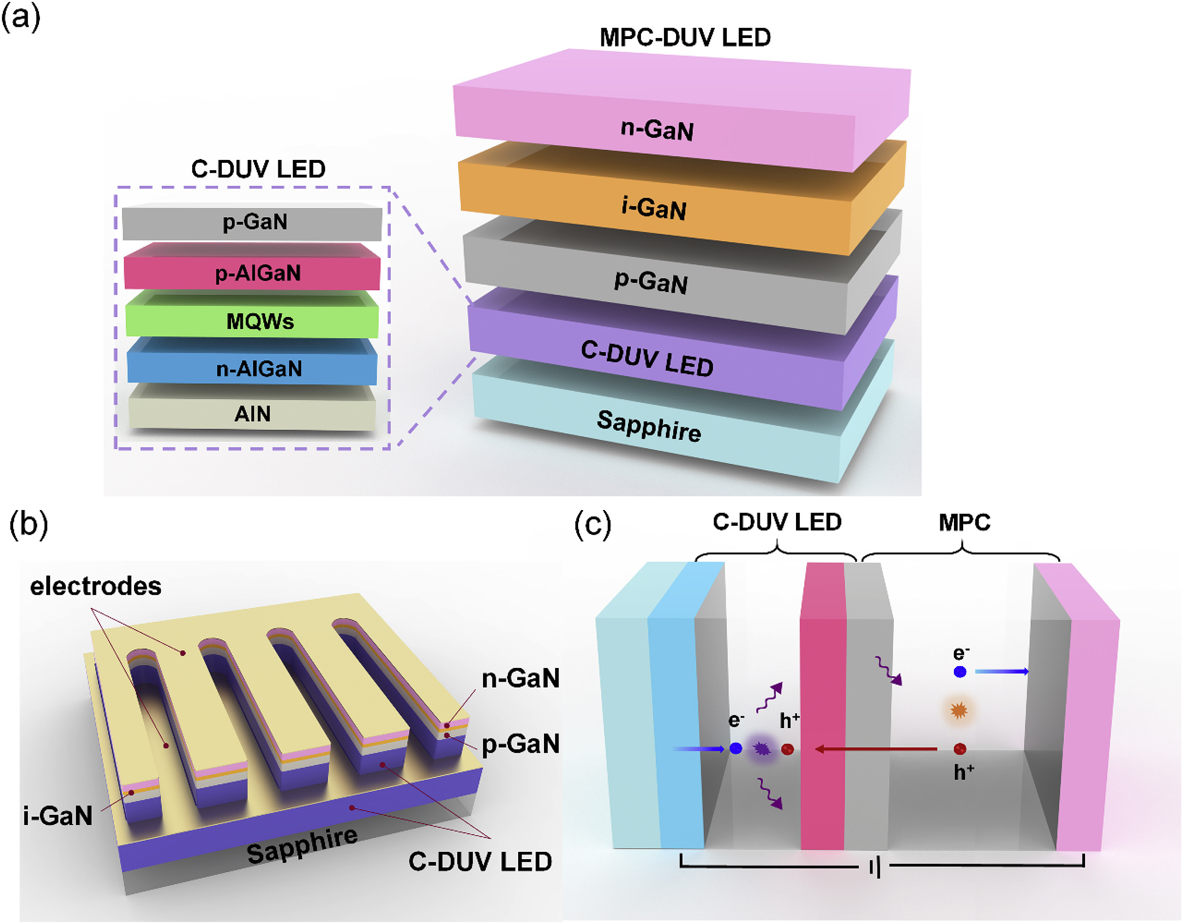
The DUV LED integrated with a multiplicative photoelectric converter (MPC) is composed of p-GaN/intrinsic GaN/n-GaN (p-i-n GaN) structure to induce the electric-optic conversion. This approach considerably improves the hole injection efficiency, as shown above in Fig.1 (a) Schematic of C-DUV LED and MPC-DUV LED, and (b)schematic device structure of MPC-DUV LED; and (c) schematic carrier recombination and generation of MPC-DUV LED.
The p-i-n GaN structure acts as a hole-multiplier first by DUV light absorption and then by electron-hole pair generation. The newly generated electron-hole pairs are firstly separated by the electric field in the p-i-n GaN structure so that multiple holes are driven into multiple quantum wells (MQWs), and finally contribute to the radiative recombination.
The team demonstrated that under low excitation, the C-DUV LED is a current-driven device while the MPC-DUV LED is more likely a voltage-driven device. For the identical output power of 33.0 μW demonstrated as point A in Fig. 2 (below), the driving current and voltage of C-DUV LED and MPC-DUV LED are 4.88 V, 1.87 mA and 19.5 V, 7.85 μA, respectively. Accordingly, the WPE of these two kinds of DUV LEDs are 0.36 percent and 21.6 percent, respectively, which shows a 60 times enhancement.

Fig. 2 EL spectra for (a) the C-DUV LED, and (b) the MPC-DUV LED. (c) Light output power for the MPC-DUV LED and the C-DUV LED.
The research further revealed the mechanism of the high WPE. By APSYS simulation, the electric field in i-GaN layer is as high as 5×10⁶ V/cm, which surpasses the threshold (2.4~2.8×10⁶ V/cm) to trigger Geiger mode multiplication in GaN, which realise a tens or hundreds of times of multiplication for the carriers. The process of photon recycle mechanism is demonstrated as shown in Fig. 3 (below).
First, half of the DUV photons propagate into the n-AlGaN layer, which can escape successfully from the bottom of the sapphire. Then the other half of the DUV photons propagate towards the MPC structure and are almost absorbed by the i-GaN layer of the MPC structure. The photons with short wavelengths can excite free carriers. The excited electrons drift towards the p-electrode under the external electric field, and collide with other atoms for ionizing more carriers. The simultaneously generated holes can be re-injected into the MQWs for contributing the radiative recombination. As a result, the MPC-DUV LED can realise a significant carrier injection efficiency.

Fig. 3 (a) Electric field profile across the MPC layers in the MPC-DUV LED at the bias level of 6 V. (b) Photon recycle, gain and output process for the MPC-DUV LED.
This work proposed a novel approach to realise highly-efficient DUV LED by monolithic integration of DUV LED with an MPC (p-i-n GaN) structure to achieve a very high WPE of 21.6 percent.
'Monolithic integration of deep ultraviolet LED with a multiplicative photoelectric converter' by Shuai Wang et al; Nano Energy 9th October 2019


