
Japanese team develops new GaN crystal manufacturing device
THVPE method forms high-quality crystals at a faster growth rate with fewer dislocation defects
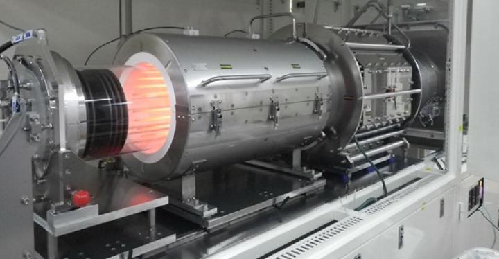
The Japan Science and Technology Agency (JST) has announced the successful development of a high-quality bulk GaN growth device based on the THVPE method, a development topic of the Newly extended Technology transfer Program (NexTEP).
Development towards commercial applicability was carried out by the Innovation and R&D Division of Taiyo Nippon Sanso from August 2013 to March 2019, based on the research of Akinori Koukitsu of the Tokyo University of Agriculture and Technology. The research team has developed a GaN crystal manufacturing device that achieves high speed, high quality, and continuous growth.
The majority of GaN crystal substrates used in electronic devices are manufactured using the Hydride Vapour Phase Epitaxy (HVPE) method. It is difficult to produce thick GaN crystals using the HVPE method due to distortions in the crystal, and GaN crystals are grown on a seed crystal heterogeneous substrate, and repeatedly peeled off at a thickness of less than 1mm for use. For this reason, commercially practical manufacturing of GaN crystals has not been possible thus far on the basis of cost and crystal quality, particularly in light of the pre- and post-work required in the process, such as cleaning the furnace.
Taiyo Nippon Sanso has advanced the HVPE method to develop a GaN crystal production system that achieves high-speed, high-quality, continuous growth through the Tri-halide Vapor Phase Epitaxy (THVPE) method using a gallium trichloride-ammonia reaction system. The THVPE method succeeds in forming high-quality crystals at a high-speed growth rate three times faster than current conventional methods, with only one-fifth the current rate of dislocation defects.
The new THVPE method also offers many cost advantages over current techniques, such as not deteriorating quartz glass tube as the reactor, preventing reduction of crystal growth area, and reducing the occurrence of unnecessary polycrystals.
If the THVPE technique can be further developed to achieve production of thick GaN crystals, it will allow the mass-production of GaN crystal substrates through slicing. The new technique holds strong promise to achieve a breakthrough in the development of low-cost, high-performance GaN devices.


