
Plessey develops native Red InGaN microLEDs on silicon
Company can make native Blue, Green and Red InGaN material or tune wavelengths from 400 - 650 nm using its GaN on silicon platform
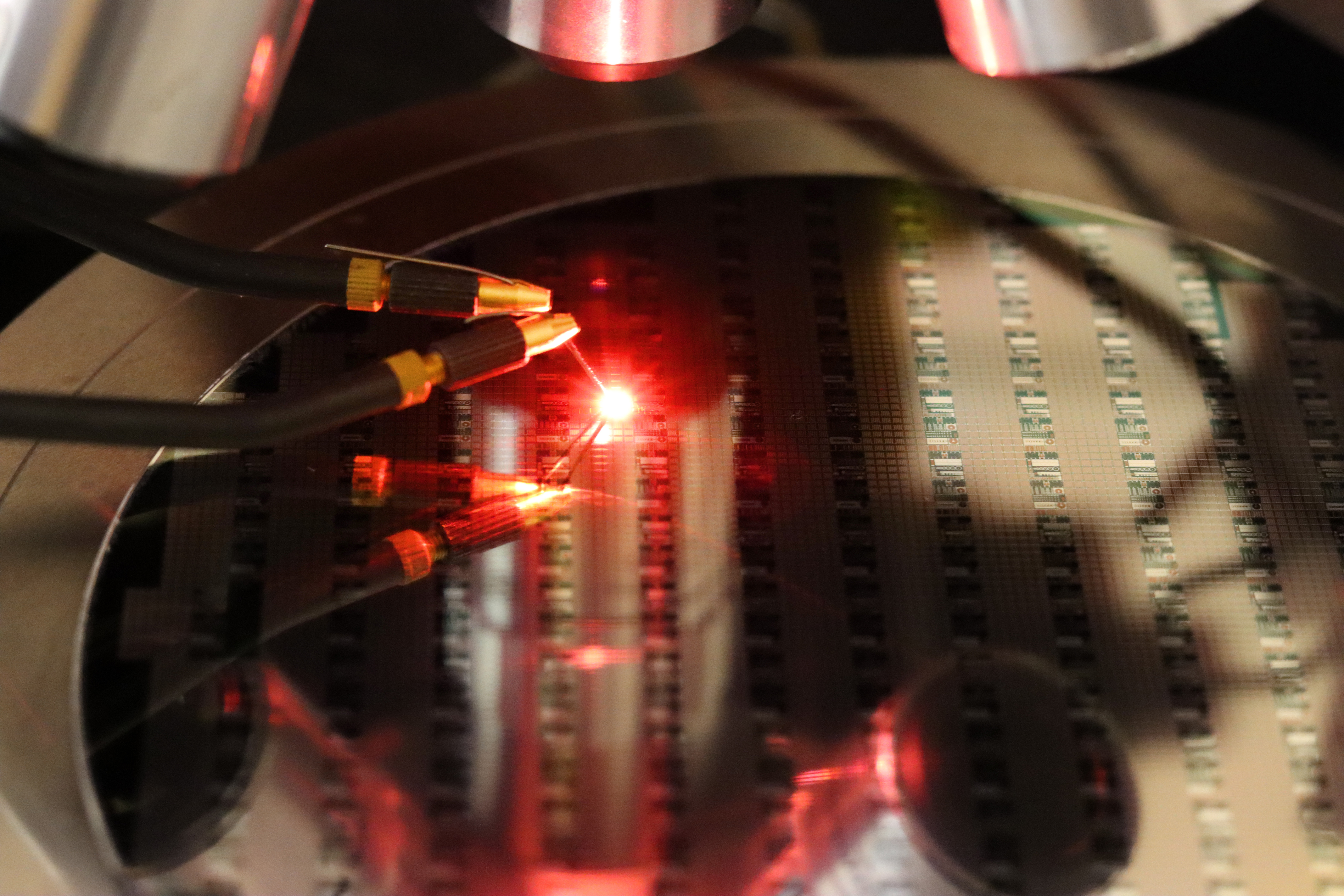
UK-based MicroLED company Plessey has successfully developed what it believes is the world's first InGaN on silicon-based Red LED.
InGaN-based Blue and Green LEDs are commercially available, Red LEDs are typically based on AlInGaP material or colour converted Red. For AR, achieving high efficiency ultra-fine pitch Red pixels (< 5 µm) remains elusive due to severe edge effects from AlInGaP material and cavity losses from colour conversion processes.
InGaN-based Red is attractive as it offers lower manufacturing costs, scalability to larger 200 mm or 300 mm wafers and better hot/cold factor over incumbent AlInGaP-based Red. However, achieving red spectral emission with InGaN material is challenging due to the high indium content inducing significant strain in the active region, subsequently reducing crystal quality and creating numerous defects.
Plessey has successfully overcome these challenges by using a proprietary strain engineered active region to create an efficient InGaN Red LED.
Plessey’s InGaN Red microLEDs have a wavelength of 630 nm at 10 A/cm2, full width at half maximum of 50 nm, hot cold factor over 90 percent and higher efficiencies over conventional AlInGaP and colour converted Red at ultra-fine pixel pitches. With this result, Plessey now has the capability to manufacture native Blue, Green and Red InGaN material or tune wavelengths from 400 - 650 nm using its GaN on Silicon platform.
Wei Sin Tan, Director of Epitaxy and Advanced Product Development, at Plessey, said: “This is an exciting result as it creates a path towards low cost manufacturing of ultra-fine pitch and efficient Red InGaN pixels, which will accelerate the adoption of microLEDs in both AR microdisplays and mobile/large display applications. Our innovative solutions have once again proven Plessey’s position as the world leader in microLED technology.”
Other recent milestones from Plessey includes the world’s first wafer level bonded monolithic 3,000 ppi GaN on Silicon microLED emissive display hybridised to an active-matrix CMOS backplane; as well as native Blue and Green emission layers on the same wafer.


