
NUS team develops large area, flexible perovskite IR LEDs
High-efficiency LEDs cover an area of 900 mm2 using low-cost solution-processing methods
Infrared LEDs are conventionally useful for optical communications and covert illumination, and are commonly found in remote controls and security camera setups. They are generally small point sources, which limits their use if larger-area illumination is required in close proximity, for instance on a wearable device.
Now National University of Singapore researchers have developed highly efficient, large-area and flexible near-infrared LEDs for new wearable device technologies.
The team led by Tan Zhi Kuang from the Department of Chemistry and the Solar Energy Research Institute of Singapore (SERIS), NUS has developed high-efficiency near-infrared LEDs which can cover an area of 900 mm2 using low-cost solution-processing methods. This is several orders of magnitude larger than the sizes achieved in other reports, and opens up a range of new applications.
Their devices employ a perovskite-based semiconductor. By using a new device architecture, the research team is able to precisely tune the injection of electrons and holes (negative and positive charges) into the perovskite, such that a balanced number of opposite charges could meet and give rise to efficient light generation. The team also found that this improvement allowed large-area devices to be made with significantly higher reproducibility.
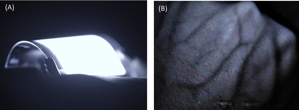
Figure (A) shows uniform electroluminescence from a large-area flexible perovskite light-emitting diode developed by the research team. Figure (B) shows illumination with near-infrared perovskite light-emitting diode on the back of the fist. This allows for the imaging of subcutaneous blood vessels. [Credits: Nature Photonics]
Zhao Xiaofei, a PhD student on the research team said: “We found that the hole-injection efficiency is a significant factor that affects the performance of the devices. By using an organic semiconductor with a shallower ionisation potential as part of the device structure, we were able to improve the hole injection and achieve charge balance. This allowed our devices to emit light at efficiencies (external quantum efficiency of 20%) close to their theoretical limit, and additionally reduced the device-to-device performance variation, hence enabling the realisation of much larger devices.”
Tan said, “Some of the technologies that our device could enable may include covert illumination in facial recognition or augmented reality/virtual reality eye-tracking technologies. In particular, we have demonstrated that our LEDs could be suited for applications involving subcutaneous deep-tissue illumination, such as in wearable health-tracking devices.”
“These materials could also be developed to emit light in the full range of visible colours. They could therefore be applied in newer generations of flat-panel electronic displays,” he added.
'Large-area near-infrared perovskite light-emitting diodes' by X Zhao; ZK Tan; Nature Photonics 2019.


