
Imec shows Scalable III-V and III-N Devices on Silicon
GaAs and GaN devices on silicon will enable 'beyond 5G' RF front-end modules
Imec, the Belgian research and innovation hub, has presented the first functional GaAs-based heterojunction bipolar transistor (HBT) devices on 300mm Si, and CMOS-compatible GaN-based devices on 200mm Si for mm-wave applications.
The results demonstrate the potential of both III-V-on-Si and GaN-on-Si as CMOS-compatible technologies for enabling RF front-end modules for beyond 5G applications. They were presented at last year’s IEDM conference (Dec 2019, San Francisco) and will be featured in a keynote presentation of Imec’s Michael Peeters about consumer communication beyond broadband at IEEE CCNC (10-13 Jan 2020, Las Vegas).
In wireless communication, with 5G as the next generation, there is a push towards higher operating frequencies, moving from the congested sub-6GHz bands towards mm-wave bands (and beyond). The introduction of these mm-wave bands has a significant impact on the overall 5G network infrastructure and the mobile devices. For mobile services and Fixed Wireless Access (FWA), this translates into increasingly complex front-end modules that send the signal to and from the antenna.
To be able to operate at mm-wave frequencies, the RF front-end modules will have to combine high speed (enabling data-rates of 10Gbps and beyond) with high output power. In addition, their implementation in mobile handsets puts high demands on their form factor and power efficiency. Beyond 5G, these requirements can no longer be achieved with today’s most advanced RF front-end modules that typically rely on a variety of different technologies amongst others GaAs-based HBTs for the power amplifiers – grown on small and expensive GaAs substrates.
“To enable the next-generation RF front-end modules beyond 5G, Imec explores CMOS-compatible III-V-on-Si technology”, says Nadine Collaert, program director at Imec. “Imec is looking into co-integration of front-end components (such as power amplifiers and switches) with other CMOS-based circuits (such as control circuitry or transceiver technology), to reduce cost and form factor, and enabling new hybrid circuit topologies to address performance and efficiency. Imec is exploring two different routes: (1) InP on Si, targeting mm-wave and frequencies above 100GHz (future 6G applications) and (2) GaN-based devices on Si, targeting (in a first phase) the lower mm-wave bands and addressing applications in need of high power densities. For both routes, we have now obtained first functional devices with promising performance characteristics, and we identified ways to further enhance their operating frequencies.”
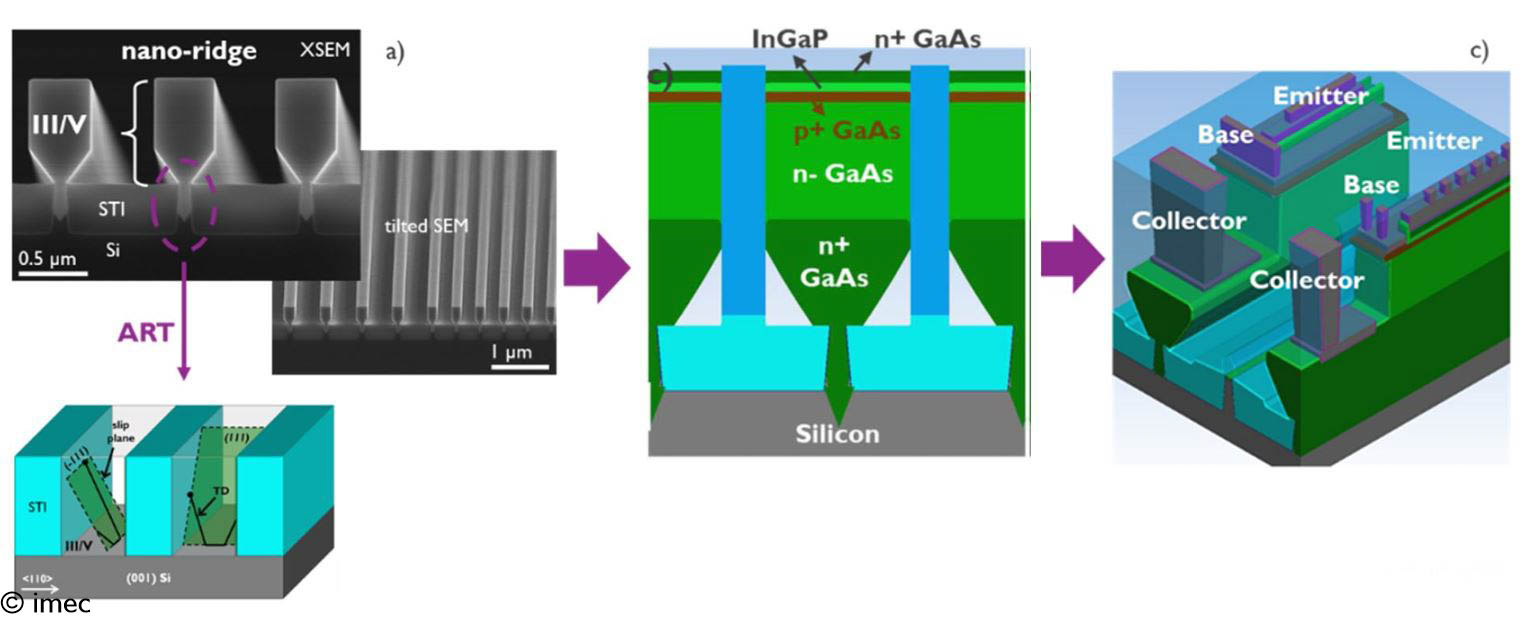
Functional GaAs/InGaP HBT devices grown on 300mm Si have been demonstrated as a first step towards the enablement of InP-based devices. A defect-free device stack with below 3x106cm-2 threading dislocation density was obtained by using Imec’s unique III-V nano-ridge engineering (NRE) process. The devices perform considerably better than reference devices, with GaAs fabricated on Si substrates with strain relaxed buffer (SRB) layers. In a next step, higher-mobility InP-based devices (HBT and HEMT) will be explored.
The image above shows the NRE approach for hybrid III-V/CMOS integration on 300mm Si: (a) nano-trench formation; defects are trapped in the narrow trench region; (b) HBT stack growth using NRE and (c) different layout options for HBT device integration.
Moreover, CMOS-compatible GaN/AlGaN-based devices on 200mm Si have been fabricated comparing three different device architectures – HEMTs, MOSFETs and MISHEMTs. It was shown that MISHEMT devices outperform the other device types in terms of device scalability and noise performance for high-frequency operation. Peak cut-off frequencies of fT/fmax around 50/40 were obtained for 300nm gate lengths, which is in line with reported GaN-on-SiC devices. Besides further gate length scaling, first results with AlInN as a barrier material show the potential to further improve the performance, and hence, increase the operating frequency of the device to the required mm-wave bands.


