Loading...
News Article

UMS PDKs support PathWave Electro thermal capability

News

Foundry customers using Keysight PathWave tool can get full electro-thermal simulation of GaN and GaAs MMICs

United Monolithic Semiconductors (UMS) has announced that its 0.25μm GaN (GH25) PDK for Keysight Technologies' PathWave ADS (Advanced Design System) is now supporting the new Electro-Thermal capability (ETH) offered with PathWave ADS.

This new functionality is not only included on the GH25 GaN PDK but also on UMS PPH15X-20 GaAs power pHEMT process PDK.

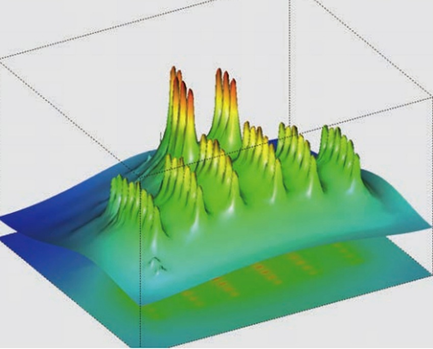
Designing packaged high power Amplifiers is a challenging task. GaAs and GaN devices concentrate high dissipated power on a very small area. Temperature rises according to the CW or pulsed conditions of use and the different materials constituting the package and assembly process used. In addition, the temperature inside the transistor impacts its properties and performance.

ADS’s Thermal simulation coupled with its Electrical simulation allows a full and complete analysis of the electro-thermal behaviour of the device and the optimisation of the MMIC inside its package. It is the appropriate design method to extract the best performance from the RF GaN devices, according to the company.

Foundry customers can get the full electro-thermal simulation of their systems by specifying thermal parameters of their own assembly solution.

This provides an elegant method to simplify the calculation of the junction temperature which is a critical step of MMIC design assessment. Implementation of thermal data in our PDKs has been possible thanks to a strong partnership with Keysight experts and development teams.

UMS says: "The partnership with Keysight is a key element which contributes to our foundry customers satisfaction through regular innovative upgrades of the MMIC design tools."

SiC MOSFETs: Understanding the benefits of plasma nitridation
Wolfspeed reports Q2 results
VueReal secures $40.5m to scale MicroSolid printing
Mitsubishi joins Horizon Europe's FLAGCHIP project
Vishay launches new high voltage SiC diodes
UK team leads diamond-FET breakthrough
GaN adoption at tipping point, says Infineon
BluGlass files tuneable GaN laser patents
QD company Quantum Science expands into new facility
Innoscience files lawsuit against Infineon
Riber revenues up 5% to €41.2m
Forvia Hella to use CoolSiC for next generation charging
Photon Design to exhibit QD simulation tool
Ortel transfers CW laser fabrication to Canada
Luminus adds red and blue multi-mode Lasers
PseudolithIC raises $6M for heterogeneous chiplet tech
Mesa sidewall design improves HV DUV LEDs
IQE revenue to exceed expectations
'Game-changing' VCSEL system targets clinical imaging
German start-up secures finance for SiC processing tech
Macom signs preliminaries for CHIPS Act funding
IQE and Quintessent partner on QD lasers for AI
EU funds perovskite tandems for fuel-free space propulsion
EU to invest €3m in GeSi quantum project
Transforming the current density of AlN Schottky barrier diodes
Turbocharging the GaN MOSFET with a HfO₂ gate
Wolfspeed launches Gen 4 SiC MOSFET technology
Report predicts high growth for UK's North East
Element Six unveils Cu-diamond composite
SemiQ launches hi-rel 1700V SiC MOSFETs
Lynred to exhibit Eyesential SWIR sensor for machine vision
Thorlabs buys VCSEL firm Praevium Research
×
Search the news archive

To close this popup you can press escape or click the close icon.
Logo
x
Logo
×
Register - Step 1

You may choose to subscribe to the Compound Semiconductor Magazine, the Compound Semiconductor Newsletter, or both. You may also request additional information if required, before submitting your application.


Please subscribe me to:


You chose the industry type of "Other"

Please enter the industry that you work in: