GaN-on-silicon IP landscape is changing

Historical players are stepping back, leading to a reconfiguration of the ecosystem, says KnowMade
2015-2020 period has shown decisive changes within the GaN-on-Si landscape, according to the latest report 'GaN-on-Silicon Patent-Landscape Analysis', from KnowMade, part of the Yole Group.
In 2015, Toshiba’s withdrew from the white LED market and Infineon acquired International Rectifier (IR). At that time, Toshiba and IR were leading the GaN-on-Si patent landscape, while several historical IP players including Panasonic, Sanken Electric, Toyoda Gosei, had slowed down their patenting activity.
After IR, Transphorm, Panasonic and GaN Systems started sampling and commercialising their first GaN-on-Si power devices between 2010 and 2015, a second wave of companies entered the field. These included ON Semiconductor, Dialog, Navitas, VisIC. More companies, such as STMicroelectronics, are expected soon, demonstrating the growing interest for GaN-on-Si technology in the power electronics business.
Intel and Macom: RF IP leaders
“Intel and Macom are leading the GaN-on-Si patent landscape for RF electronics applications,”says Remi Comyn, Compound Semiconductors and Electronics at KnowMade.
Intel’s RF GaN-on-Si patent portfolio mainly relates to III-N transistors used in SoC , RF switches, ultra-short channel lengths, field plates, and III-N/Silicon monolithic IC . Still, about 75 percent of Intel’s portfolio are composed of pending patent applications distributed mainly between USA with 17 patents and Taiwan with 20 patents.
Fujitsu with more than 40 patents and Macom with more than 20 patents for its side, are leading the patent landscape in terms of enforceable IP in the field of GaN-on-Si RF. Fujitsu’s portfolio focused on GaN-on-Si materials, especially on buffer layers, with inventions that might be implemented on others substrates including SiC or for other applications. Likewise Intel, Fujitsu has adopted a global patenting strategy.
In contrast Macom’s portfolio is more focused on GaN-on-Si devices for RF, addressing specific technological challenges at epitaxy, device, module and package levels. For instance, a strong patenting effort was made in 2015 in order to address the parasitic channel via counter dopants in HEMT epi-structures.
KnowMade’s analysts identified more than ten related patent applications in its new GaN-on-Silicon patent analysis. Furthermore, Macom’s patenting activity related to GaN-on-Si is essentially focused on US, although it has now requested foreign extensions for a significant number of newly published inventions.
Power electronics
Regarding power electronics, Rémi Comyn from KnowMade comments: “The growing interest in GaN-on-Si technology for power applications has not translated into a remarkable acceleration of the patenting activity. However, we observed a steady patenting activity from Infineon following IR’s acquisition, and a remarkable strengthening of Transphorm’s portfolio after Fujitsu’s decision to transfer its power supplies businesses to the US startup”.
Transphorm’s IP position has been further reinforced following the licensing agreement established in 2014 with Furukawa Electric, a key IP player in GaN-on-Si patent landscape. Likewise, Infineon Technologies closed an important IP licensing agreement with another historical player of GaN-on-Si and power electronics patent landscapes, Panasonic. STMicroelectronics, announced in 2018 an extensive R&D program in collaboration with CEA Leti a well-positioned player in the GaN-on-Si patent landscape.
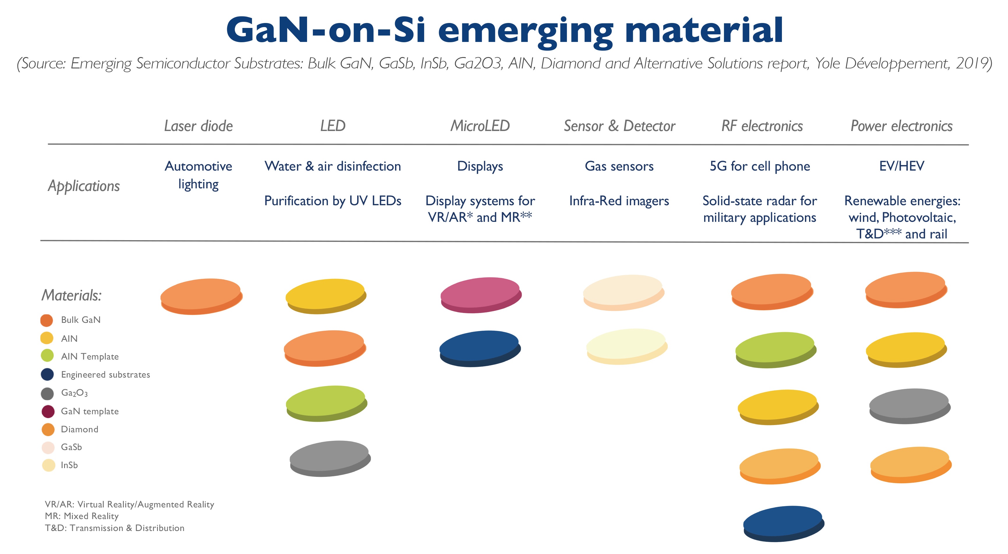
From a technical point of view, Ezgi Dogmus, technology & market analyst Compound Semiconductors & Emerging Materials at Yole asserts: “Over the last years, in the power electronics industry, we have witnessed an increasing interest for GaN HEMTs, which bring attractive performance and cost-competitive compared to Si MOSFETs. In addition to innovative start-up companies, almost all integrated device manufacturers in the Power Electronics business propose currently GaN-on-Si devices enabling systems with higher power, higher efficiency and smaller foot print than their Si MOSFET solutions.”
In power electronic sector, GaN -on-Si devices are direct competitors of Silicon SJ MOSFETs at medium voltage.
“SJ MOSFETS are still cost effectives and technologically interesting,” explains Elena Barbarini, Head of Department Devices at System Plus Consulting. “But the increase of players as the development of attractive performances at GaN epitaxy level drove an acceleration of available solutions. Its regards die design, driver integration and packaging.”
MicroLED activities
Another interesting application is the increasing GaN-on-Si activity within the microLED activities is step by step becoming more attractive and leads to huge volume opportunities.
As of 2019, a significant contribution to the patenting activity (in terms of new inventions) stems from the development of a low cost and scalable GaN-on-Si nanowires-based microLED technology, which are promising for the next-generation display technology and smart lighting applications. Most microLEDs related patents included in the landscape are related to the fabrication of GaN nanostructures.
Eric Virey, principal analyst, Technology & Market, Displays at Yole tells us the story: “The technology was first developed and patented by glō between 2010 and 2016. However, glō’s patenting activity does not put the emphasis on GaN-on-Si, although it is a preferred embodiment”.
In parallel, since 2014, CEA and Aledia started patenting their own – jointly developed – technology with numerous requests for extending its priority patents worldwide indicating a global IP strategy/competition.
In this dynamic ecosystem, GaN-on-Si technologies look attractive and promising.


