
New threads: BN Nanotubes hold promise for wearables
By encasing tellurium nanowires like a straw, BN nanotubes could be controllable by light and pressure
Wearable tech and electronic cloth may be the way of the future, but to get there the wiring needs to be strong, flexible and efficient.
Boron nitride nanotubes (BNNT), studied by physicists at Michigan Technological University, encase tellurium atomic chains like a straw, which could be controllable by light and pressure. In collaboration with researchers from Purdue University, Washington University and University of Texas at Dallas, the team have published their findings in Nature Electronics.
As demand for smaller and faster devices grows, scientists and engineers turn to materials with properties that can deliver when existing ones lose their punch or can't shrink enough.
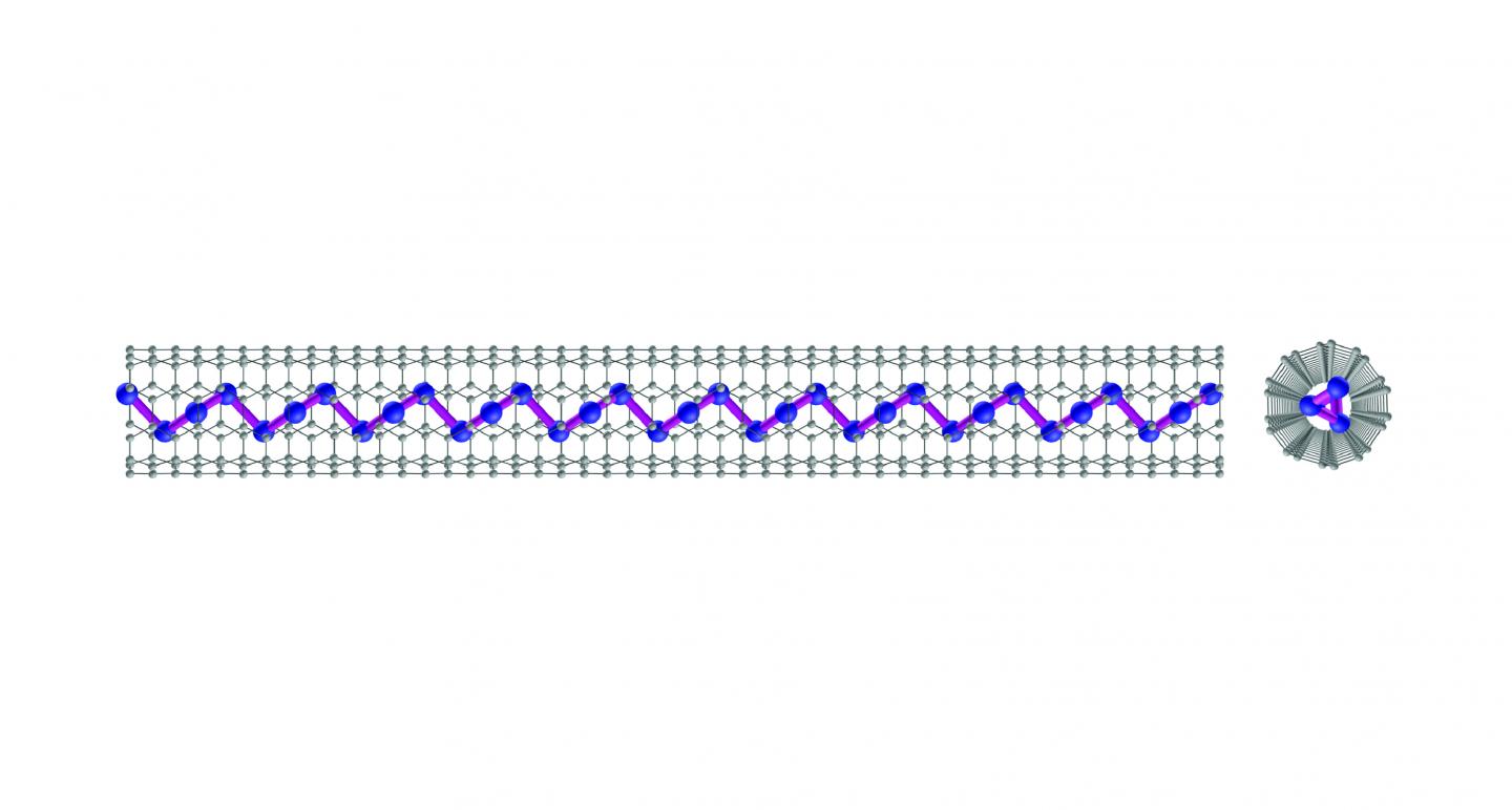
BNNTs are highly insulating as well as being strong and bendy. This makes them a good candidate to pair with another material with great electrical promise: tellurium. Strung into atom-thick chains, and threaded through the hollow centre of BNNTs, tellurium atomic chains become a nanowire with immense current-carrying capacity.
"Without this insulating jacket, we wouldn't be able to isolate the signals from the atomic chains. Now we have the chance to review their quantum behaviour," Yap said. "The is the first time anyone has created a so-called encapsulated atomic chain where you can actually measure them. Our next challenge is to make the boron nitride nanotubes even smaller."
A bare nanowire is kind of a loose cannon. Controlling its electric behaviour -- or even just understanding it -- is difficult at best when it's in rampant contact with flyaway electrons. Nanowires of tellurium, which is a metalloid similar to selenium and sulphur, is expected to reveal different physical and electronic properties than bulk tellurium. Researchers just needed a way to isolate it, which BNNTs now provide.
"This tellurium material is really unique. It builds a functional transistor with the potential to be the smallest in the world," said Peide Ye, the lead researcher from Purdue University, explaining that the team was surprised to find through transmission electron microscopy at the University of Texas at Dallas that the atoms in these one-dimensional chains wiggle. "Silicon atoms look straight, but these tellurium atoms are like a snake. This is a very original kind of structure."
The tellurium-BNNT nanowires created field-effect transistors only 2 nm wide; current silicon transistors on the market are between 10 to 20 nanometers wide. The new nanowires current-carrying capacity reached 1.5x108 cm2, which also beats out most semiconducting nanowires. Once encapsulated, the team assessed the number of tellurium atomic chains held within the nanotube and looked at single and triple bundles arranged in a hexagonal pattern.
Additionally, the tellurium-filled nanowires are sensitive to light and pressure, another promising aspect for future electronics. The team also encased the tellurium nanowires in carbon nanotubes, but their properties are not measurable due to the conducting or semiconducting nature of carbon.
Before people begin sporting tellurium T-shirts and BNNT-laced boots, the nature of these atomic chains needs characterising before its full potential for wearable tech and electronic cloth can be realised.


