
ZSW to delve further into Solar Cell Anatomy
Researchers hope new scanning electron microscope will reveal more about the surface structures of CIGS and perovskite solar cells
Scientists at the Centre for Solar Energy and Hydrogen Research Baden-Württemberg (ZSW) now have a far more powerful tool to better investigate solar cells – a new scanning electron micro-scope.
In full operation since January 2020, this device has twice the resolution of its predecessor and the ability to image structures measuring just a few nanometers. Its focused ion beam cuts cross-sections of layers smoothly and precisely.
Researchers aim to gain a better understanding of thin-film solar cells’ structure and interfaces on a nanoscale. They also want to gain deeper insights into defects. This knowledge is crucial to the solar industry’s efforts to assure quality and continue to boost solar cells’ efficiency. More efficient solar cells can further shrink photovoltaic systems’ small CO2 footprint and boost PV’s contribution to mitigating climate change.
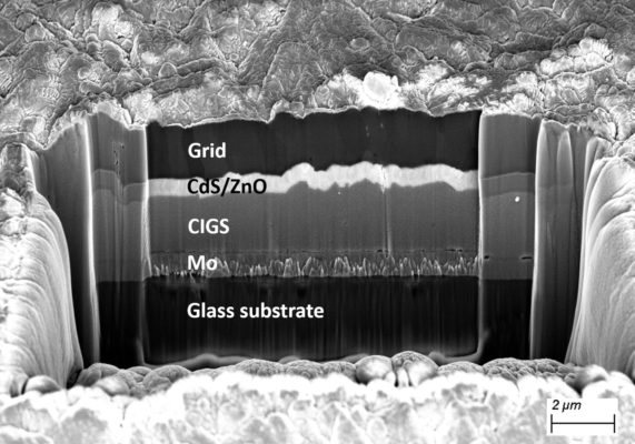
High-resolution scanning electron microscopes are excellent analytical instruments for developing thin-film solar cells based on CIGS and other solar cells such as perovskites. These tools furnish information about layer growth and thickness, morphology and chemical composition. They scan with an electron beam and render the smallest surface structures in three-dimensional images. The picture above shows a cross-section of a CIGS thin-film solar cell with the new scanning electron microscope. Such pictures will help spot undesirable cavities and foreign particles in the materials, according to the researchers.
Nanoscale views for more nuanced observations
The new FIB-SEM at the ZSW is able to detect image points less than a nanometer apart. Solar cells’ structures are clearly visible down to a scale of ten nanometers, or 0.00001 mm. “The device opens up new possibilities for us in the investigation of thin-film solar cells,” says Theresa Friedlmeier, group leader Analytics and Simulation at the ZSW Department of Photovoltaics: Materials Research. “We can now analyse the shape and size of particles and inclusions, and investigate micro-areas using energy dispersive X-ray spectroscopy.”
The new device can serve to examine the very thin interface between the CIGS and the buffer layer of CdS with far greater depth and precision. This interface has a major impact on solar cell efficiency.
Improved sample preparation with a focused ion beam
With its focused ion beam, the new scanning electron microscope en-ables researchers to prepare materials on a nanoscale. “For example, we can use it to prepare good cross-sections of CIGS solar cells on flexible substrates without damaging or separating the individual layers, which had been very difficult in the past,” says Friedlmeier. “It helps us to deepen our understanding of solar cells and develop improved processes with higher efficiencies and lower costs.” The state of Baden-Württemberg funded this new acquisition with a €650,000 grant.
The researchers will also use the new equipment to prepare the sam-ples for further investigations. These include electron backscattering, transmission electron microscopy, atom probe tomography and energy dispersive X-ray analysis.


