
Eta Research announces 4 inch Semi-Insulating GaN Wafers
Company optimistic about performance gains possible for GaN RF devices
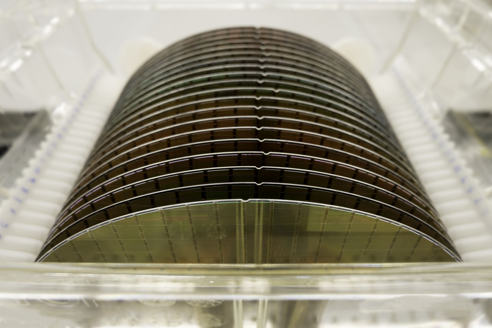
Shanghai-based Eta Research has announced the development of semi-insulating 4 inch GaN wafers, making it the first company to commercially develop such wafers at this size, it says.
Eta Research uses the HVPE method to produce GaN wafers. To compensate the unintentional n-type dopants, a deep level co-doping strategy was used to achieve high resistivity. Whereas iron doping has been the most prevalent choice for semi-insulating GaN, Eta Research uses carbon doping. SIMS data shows the carbon concentration to be in the range of 5E17 to 3E18 /cm3. The unintentional n-type dopants of oxygen and silicon are below 1E17 /cm3. The resistivity has been measured by Hall measurement and I-V curve, which result in room temperature resistivity greater than 1E9 ohm-cm.
The crystal and wafer quality specifications of the semi-insulating GaN wafers remains the same as the company’s n-type GaN wafers. XRD rocking curves of both the (002) and (102) are < 100 arcsec and typically 50 – 60 arcsec. The dislocation density has been measured by CL to be 1E6 /cm2. The lattice radius of curvature is greater than 10 m. TTV and bow can be controlled within 30 um for 100 mm wafers. The surface has an epi-ready polish with roughness < 0.3 nm for a 10 x 10 um AFM measurement and < 1.0 nm for 239 x 318 um optical interferometry measurement.
The market for semi-insulating GaN wafers is for RF HEMT devices. The RF device market is experiencing high growth due to the implementation of 5G and other wireless communication applications. GaN is a useful semiconductor material for high power and high frequency RF devices, but the industry is almost exclusively producing GaN HEMTs on SiC substrates. GaN on GaN RF devices will have lower dislocation density device layers and no buffer layer is required, so the company expects higher power and better performance will result from RF devices made on GaN substrates.
According to Eta Research’s CEO, Troy Baker; “Due to the very limited supply, size, and quality of semi-insulating GaN wafers, there has only been a limited body of research work conducted on GaN RF devices grown homoepitaxially. We plan to work with customers to prove the value proposition of GaN wafers for RF devices. We are very optimistic about the performance gains that could be made using semi-insulating GaN wafers. The wafers are currently available for sale and the company is building new HVPE reactors with carbon doping capability. In addition, we are able to provide MOCVD epi layers on GaN wafers.”
Each wafer will be shipped with a detailed wafer inspection form. Standard products are 2 inch and 4 inch wafers, and customised sizes are available as well.


