
A massive boost for UV LED efficiency
The monolithic integration of a conventional LED structure and a multiplicative photoelectric converter propels the wall-plug efficiency of deep UV LEDs emitting at 280 nm to more than 20 percent
BY Haiding Sun FROM University of Science and Technology of China AND Hanling Long, Feng wu, Jiangnan Dai and Changqing Chen FROM Huazhong University of Science and Technology
For many decades, the most common source of UV light has been the mercury lamp. It has netted substantial sales, due to its widespread use in air/water purification, sterilization, phototherapy, lithography and UV curing. However, it is a source of UV emission that is far from ideal: it consumes much energy; lamps don’t last long; and it contains mercury, which is toxic. The latter a big deal, as concerns over health continue to grow. For example, an international treaty known as the Minamata Convention on Mercury is calling for mercury-containing products to be progressively prohibited by the end of this year.
The leading environmentally-friendly, energy-efficient alternative to the mercury lamp is the UV LED. This device, which is also renowned for its small size and long lifetime, spans a spectral range from 210 nm to 360 nm by varying the aluminium content in the AlGaN quantum wells. As well as offering an alternative to the UV lamp in some applications the UV LED can also be used for new tasks (see Figure 1). This helps the device to capture even more revenue. According to market analyst Yole Développement, the market size for the UV LED will grow from $500 million in 2019 to $1 billion in 2023.
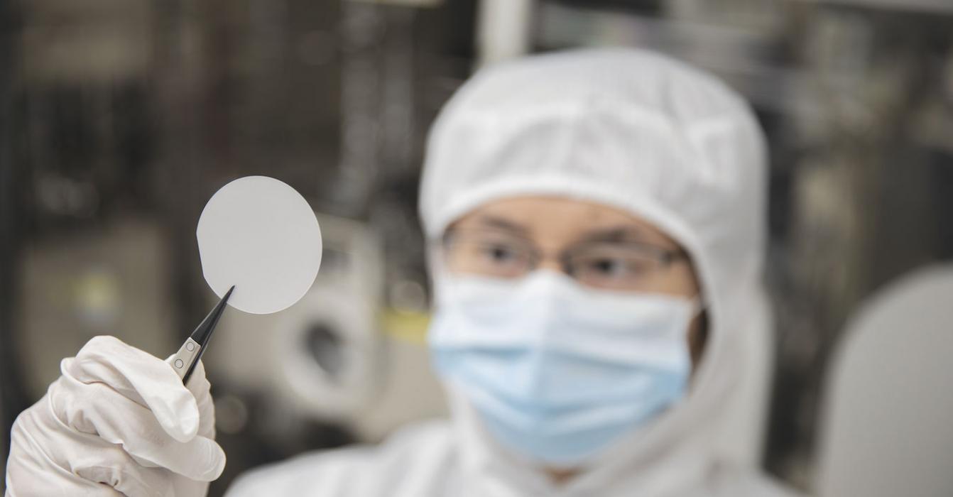
A UV LED under operation
The Achilles heel of the UV LEDs is its low efficiency. Compared to its blue cousins – which feature InGaN quantum wells, produce extremely high external quantum efficiencies and have a wall-plug efficiencies exceeding 80 percent – the performance of the UV LED is pitiful. As the wavelength drops below 360 nm efficiency plummets. For emission at 280 nm, the external quantum efficiency and wall-plug efficiency are typically just 6 percent and 5 percent, respectively.It is possible to improve efficiency by refining the device. Efficiencies increase by: reducing defects and dislocations in the epilayers; improving n- and p-type doping efficiencies, to create conductive films for better current injection; re-designing the device for better light extraction; and employing a superior AlGaN-based quantum well and barrier design in the active region.
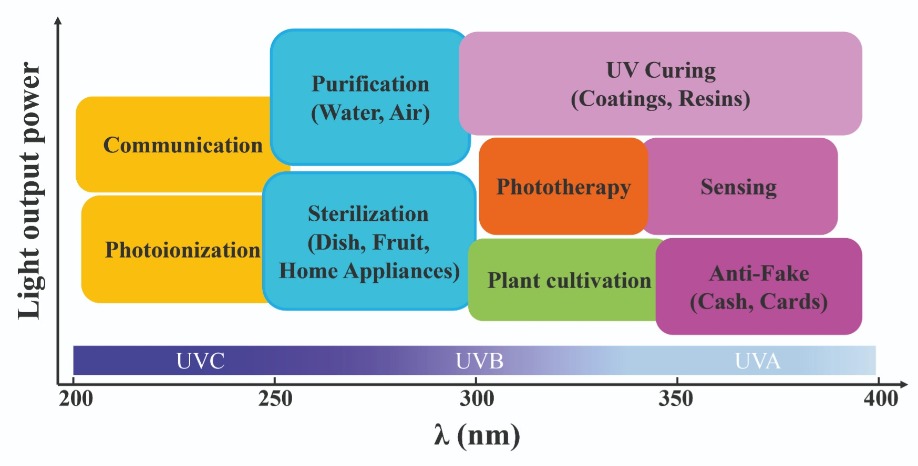
Figure 1. There are many applications for UV LEDs
Our team from the University of Science and Technology of China and Huazhong University of Science and Technology has produced more efficient UV LEDs by making much progress on all these fronts. However, this approach only gets us so far – so we have gone on to deliver a step change in performance by combining these refinements with a novel architecture that combines a conventional LED structure with a multiplicative photoelectric converter. Read on to discover the secrets of our success.Conventional strategies
We grow our heterostructures for our UV LEDs on sapphire, a low-cost transparent substrate. We avoid native AlN because it is prohibitively expensive. The downside of sapphire is that is has lattice and thermal expansion mismatch with the nitride layers, leading to an inferior crystalline quality that drags down the radiative recombination efficiency. To tackle this issue, we have turned to pyramidal patterned sapphire, a foundation that supports lateral overgrowth during AlN epitaxy. The AlN films that result have excellent crystal quality. According to the full-width at half-maximum of the peaks produced from X-ray diffraction rocking curves, the threading dislocation density is less than 3×108 cm-2 (see Figure 2 (a)). We have also undertaken reciprocal space mapping – this shows that the epilayers are free from strain. Based on these findings, we know that we can supress the density of non-radiative recombination centres in the active region of our UV LEDs, and ultimately realise a high radiative recombination efficiency in these devices.
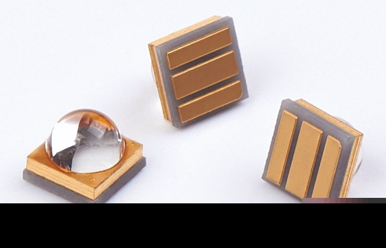
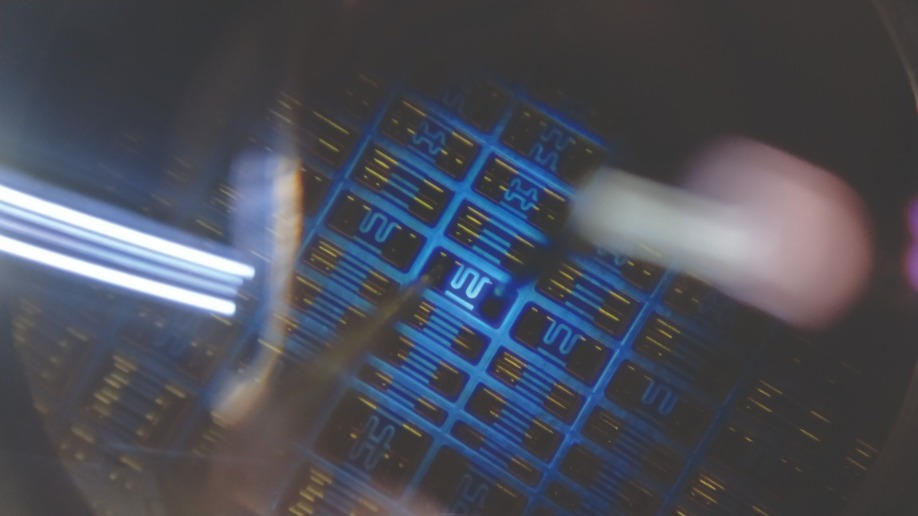
Packaged UV LEDs
The benefits of patterning a substrate are not limited to the better material quality that comes from annihilation of dislocations. In addition, texturing boosts the output from the chip. This is particularly important in the deep UV, where the optical polarisation induced by the unique valance band structure within the active region limits the light extraction from the device. Unfortunately, the transverse-electric mode, which dominates in blue LEDs and aids extraction, is overtaken by the transverse-magnetic polarisation mode.Previous work by our team has shown the benefits of using a moth-eye microstructure on sapphire’s bottom surface of a flip-chip UV LED (see Figure 2(b)). With this pattern the uniformly periodic microstructure extends the light extraction angle. Note that this particular microstructure enhances the transverse-electric mode. It has a distribution with a dominate contribution in the vertical direction, which is easier to extract.
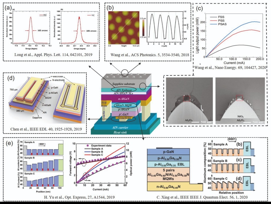
Figure 2. Strategies to improve the performance of UV LEDs. (a) Patterned sapphire substrates enhance the crystal quality of epitaxy AlN. H. Long et al. Appl. Phys. Lett. 114 042101 (2019) (b) Fabricating moth-eye microstructure on the sapphire bottom surface of flip-chip UV LEDs enlarges the light extraction angle. S. Wang et al. ACS Photonics 5 3534 (2018) (c) Switching to a patterned sapphire with silica array (PSSA) reduces the threading dislocation density and enhances light extraction efficiency, thanks to the large refractive index contrast between the epilayers and PSSA. S. Wang et al. Nano Energy 69 104427 (2020) (d) Novel electrode patterns can optimise current-spreading in a UV LED chip. Q. Chen et al. IEEE Elect. Dev. Lett. 40 1925 (2019) (e) Designing the band structure of the AlGaN quantum wells heterostructure in the active region improves radiative recombination. H. Yu et al. Opt. Express 27 A1544 (2019); Ren et al. J. Phys. D Appl. Phys. 53 073002 (2020)
We realise an additional increase in light extraction by modifying light polarisation via strain modulation in the AlGaN quantum wells. By ensuring compressive in-plane strain in the wells we promote emission of the transverse-electric mode, leading to a hike in light-extraction efficiency for the UV LED.Recently, we have made further gains by combining patterned sapphire with a silica array (see Figure 2(c)). This modification reduces threading dislocation density and enhances light extraction efficiency, thanks to a large difference in refractive index between the AlGaN epilayers and the patterned sapphire with a silica array. Another factor that governs the performance of the UV LED is how efficiently the current can be injected into the device. As sapphire is insulating, it is impractical to adopt a vertical LED architecture. Due to this, the most common design for improving current injection and light extraction is based on a flip-chip bonding technology. Unfortunately, current crowding results, deteriorating device performance.
One option that we have developed for increasing the uniformity of current spreading in UV LED chips is to introduce novel electrode patterns (see Figure 2(d)). With this design, the n-type electrode surrounds its p-type counterpart to provide sufficient current paths for carrier transport.
Last but by no means least, UV LEDs are hampered by the strong spontaneous polarisation and the piezoelectric polarisation field in the AlGaN material system. Due to the quantum confined Stark effect, the wavefunctions of the electron and hole are pulled in opposite directions, suppressing effective radiative recombination. To address this, a variety of forms of bandgap engineering have been pursued to increase the internal quantum efficiency, suppress the current leakage and diminish efficiency droop at high current injection (see Figure 2(e)).
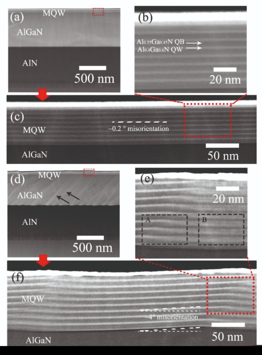
Figure 3. Cross-sectional scanning transmission electron microscopy image of AlGaN multi-quantum wells grown on (a-c) 0.2° and (d-f) 4° misoriented sapphire substrates. H. Sun et al. Adv. Funct. Mater. 29 1905445 (2019)
Part of the reason behind the high quantum efficiency of blue LEDs is the indium segregation in the InGaN quantum wells. Segregation results in carrier localisation effects, increasing the likelihood of radiative recombination. With the AlGaN quantum wells required for UV LEDs, segregation is far less pronounced, because aluminium atoms have a far lower mobility than gallium. Localisation can also result from thickness variations, but it is challenging to introduce, because aluminium and gallium atoms are a similar size.The good news is that we are able to replicate the carrier localisation effects in blue LEDs in our UV emitters with a new kind of nanoscale structure, which we refer to as wavy quantum wells. We artificially create a ‘phase separation’, leading to compositional inhomogeneities in AlGaN alloys.
We produce LEDs with these wavy quantum wells by growing aluminium-rich deep UV LEDs on misoriented sapphire substrates with a significant mis-cut angle – it is as large as 4° (see Figure 3). The 280 nm LEDs produced by this process benefit from the semi-polar template that results – it produces a reduced polarisation field, in addition to increased carrier localisation.
Measurements on these devices produce much better results than those made using flat sapphire. Photoluminescence intensity is at least ten times higher; internal quantum efficiency is six times higher at low excitation laser power, with a record result of over 90 percent; carrier lifetime is far longer, reaching 1.60 ns on 4° misoriented sapphire, compared with just 0.06 ns on 0.2° misoriented sapphire; and wafer-level output power of the UV LEDs is two-to-three times higher (see Figures 4 and 5).
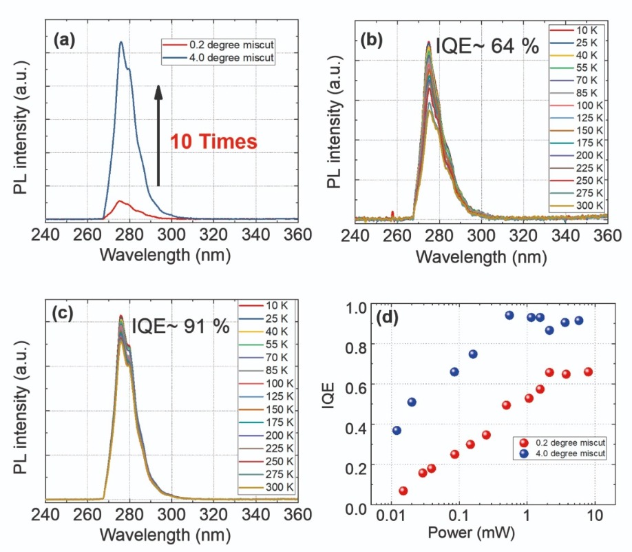
Figure 4. (a) Room-temperature photoluminescence (PL) spectra of AlGaN multi-quantum wells (MQWs) grown on 0.2° and 4° sapphire substrates. Temperature-dependent PL spectra of AlGaN MQWs grown on (b) 0.2° and (c) 4° misoriented substrates. (d) Internal quantum efficiency (IQE) as a function of pumping power for both MQWs grown on 0.2° (red dots) and 4° (blue dots) misoriented substrates. H. Sun et al. Adv. Funct. Mater. 29 1905445 (2019)
Even with this improvement to the internal quantum efficiency of the UV LED, the wall-plug efficiency is typically below 5 percent for devices emitting below 300 nm. To reach far higher values requires a radical change to the design. We have done just that, realising a record wall-plug efficiency of 21.6 percent through the monolithic integration of a deep UV LED with a multiplicative photoelectric converter.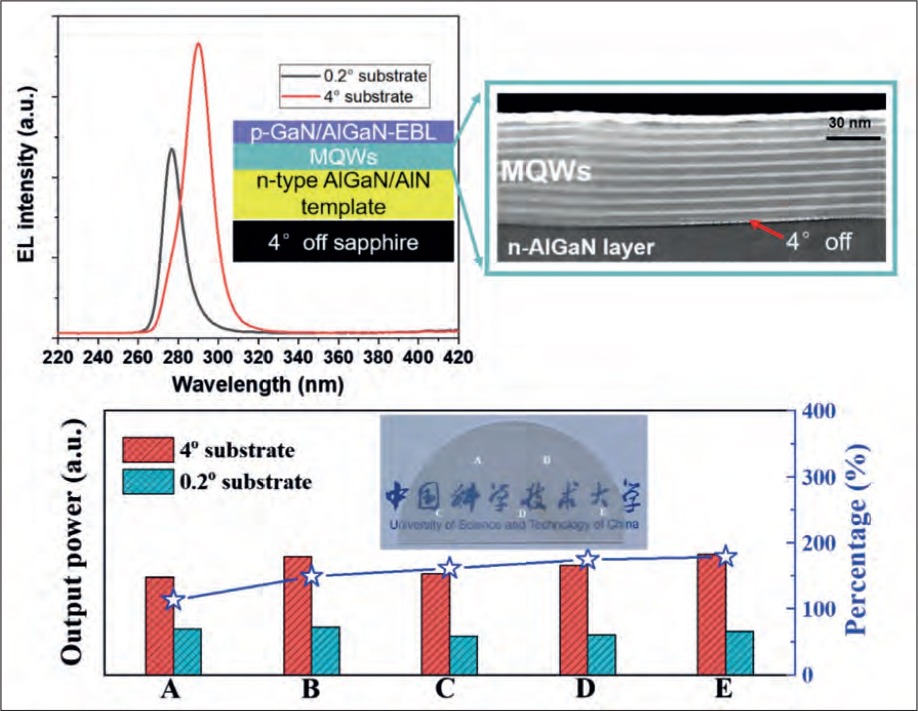
Figure 5. Electroluminescence (EL) spectra and output power comparison. H. Sun et al. Adv. Funct. Mater. 29 1905445 (2019)
A radical architectureOur novel device tackles the extremely low injection efficiency in conventional deep UV LEDs that is to blame for the unsatisfactory efficiency. In our radical design, the p-i-n GaN structure acts as an electric-optic converter and hole-multiplier, absorbing deep UV photons and generating electron-hole pairs. These carriers are pulled apart by the extremely high electric field. Holes are then multiplied by impact ionisation, before being re-injected into the active region, where they take part in radiative recombination (see Figure 6).
To investigate the photoelectric characteristics of our new device, we have compared its electroluminescence spectra to that of a conventional UV LED (see Figure 7(a) and (b)). Note that our new device exhibits a voltage-dependent characteristic, due to the reverse-biased multiplicative photoelectric converter. Plots of light output reveal an identical power when the conventional device is run at 4.88 V and 1.87 mA, and the novel LED is driven at 19.5 V and 7.85 µA. From these figures we can conclude that the wall-plug efficiency in the conventional device is 0.36 percent, while that with the photoelectric converter is 21.6 percent – that is 60 times higher.
Material deposition for device fabrication
The current-voltage characteristics are markedly different from the norm in our novel device (see Figure 8). For our conventional UV LED, turn-on is at 4.5 V, while the leakage current is very low, indicating that it is reliable. In comparison, for our record-breaking LED, there are three distinct regions that span different ranges of operating voltage (for details, see Figure 8).We have simulated the electric field profile of the p-i-n GaN region under a 6 V bias (see Figure 9(a)). Calculations reveal that the electric field extends into the n-GaN layer, and that the i-GaN layer is completely depleted. What’s more, these simulations show that the strength of the electric field exceeds 5 MV/cm, making it strong enough to realise Geiger mode multiplication in GaN material.
Our modelling also offers an insight into the operation of our LED. When deep UV photons are absorbed within the device, they generate an electron hole pair, and due to the reverse bias in the multiplicative photoelectric converter, electrons drift to the anode and holes to the cathode. Due to Geiger mode, each carrier is multiplied several dozens of times in the multiplicative photoelectric converter, before it is re-injected into the active region. This results in a significant enhancement for the hole-injection efficiency in this class of LED. Photon recycling can also take place in this device (see Figure 9(b)) for details).
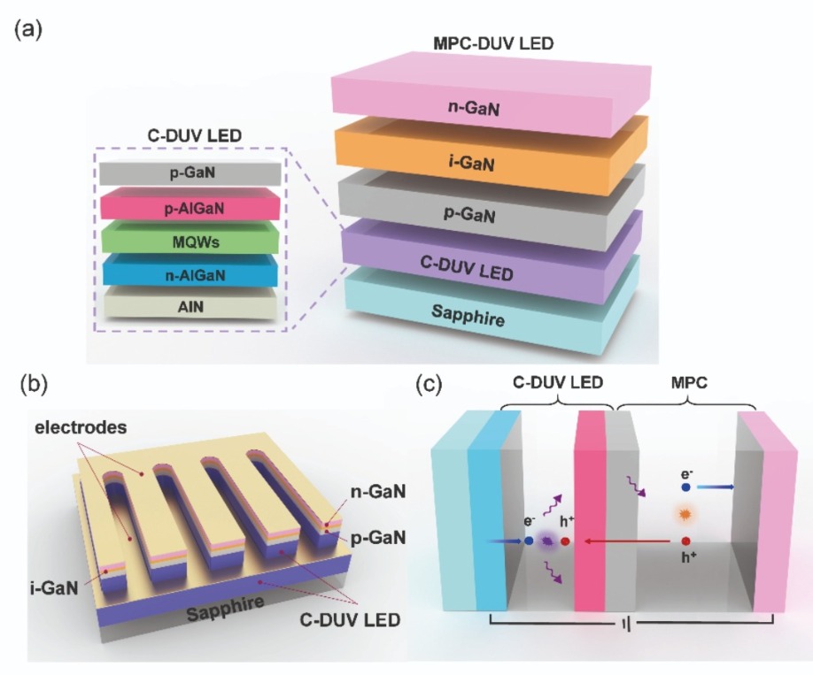
Figure 6. (a) The design of a conventional deep UV LED (C-DUV LED) and a multiplicative photoelectric converter deep UV LED (MPC-DUV LED). (b) Device structure of MPC-DUV LED. (c) An illustration of the carrier recombination and photon recycle process of the MPC-DUV LED. For more details see: S. Wang et al. Nano Energy. 66 104181 (2019).
The novel device that we have developed promises to realise far more than just a hero result in a lab. Its mass-production is not that difficult, as the multiplicative photoelectric converter can be grown in-situ using conventional MOCVD. The challenge is to improve the light output power of this form of LED.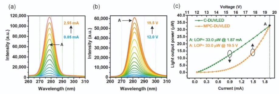
Figure 7: Electroluminescence (EL) for (a) the conventional deep UV LED (C-DUV LED), and (b) the multiplicative photoelectric converter deep UV LED (MPC-DUV LED). (c) Light output power for the MPC-DUV LED and the C-DUV LED. More details are provide in: S. Wang et al. Nano Energy. 66 104181 (2019).
Although there are applications where low-power deep UV LEDs can serve, such as microLEDs, many opportunities require sources with a high power. We are targeting this goal by optimising the epitaxial structure and fabrication process.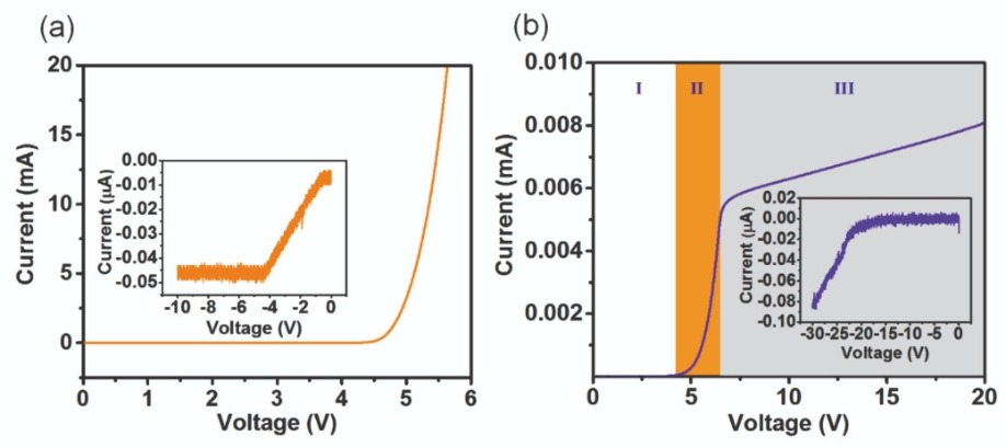
Figure 8. Current-voltage characteristics of (a) a conventional deep UV LED (C-DUV LED) and (b) a multiplicative photoelectric converter deep UV LED (MPC-DUV LED). Insets show the reverse bias conditions. For region I and II, the curve is similar to that of the C-DUV LED, however, the current level is almost three magnitudes lower. For region III, which begins at 6.6 V, the current tendency changes abruptly, indicating minority carriers are effectively suppressed by the space charge region in the p-i-n GaN structure, and that the overall current may be limited by the reverse drift current. It may be attributed to the increase in the series resistance of the p-i-n GaN structure compared to region II. For more details please see: S. Wang et al. Nano Energy. 66 104181 (2019).
While a 20 percent wall-plug efficiency is a very encouraging result, there is still much work to do. We hope that further increases in both the external quantum efficiency and the wall-plug efficiency are within our grasp by improving the material quality, the doping efficiency, and light extraction. Such efforts will take place during the on-going transition period from the mercury-based UV lamp to AlGaN-based UV LEDs, and will help to increase the adoption of clean, reliable UV sources. Given the rapid development in visible InGaN-based LEDs, all of us have good reason to be optimistic about the realisation of highly efficient, high-power deep UV LEDs in the near future.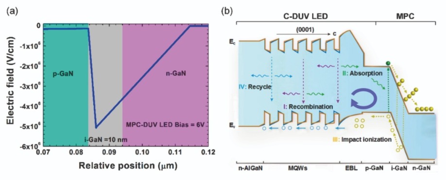
Figure 9. (a) Electric field profile across the multiplicative photoelectric converter (MPC) structure in the MPC-deep UV LED at a 6 V bias. (b) The photon recycling, gain and output process for the MPC-DUV LED. In the initial recombination process I, half of the DUV photons propagate to the n-AlGaN layer and escape successfully, as shown by the purple arrows. The other half of the DUV photons propagate towards the MPC structure, and almost all are absorbed by the i-GaN layer of the MPC structure, indicated by the green arrows. DUV photons are absorbed and generate new electron-hole pairs, as shown in process II. In process III, carriers are multiplied under Geiger mode, and collide with other atoms, ionising more carriers. The multiplied holes are re-injected into the multi-quantum wells (MQWs), and contribute to new radiative recombination, as shown in process IV. Note that for conventional DUV LEDs, only steps I and II take place. More details are provided in: S. Wang et al. Nano Energy. 66 104181 (2019).
H. Sun et al. Adv. Funct. Mater. 29 1905445 (2019)
Ren et al. J. Phys. D Appl. Phys. 53 073002 (2020)
H. Yu et al. Opt. Express 27 A1544 (2019)
S. Wang et al. Nano Energy 69 104427 (2020)
S. Wang et al. Nano Energy 66 104181 (2019)
H. Long et al. Appl. Phys. Lett. 114 042101 (2019)
Q. Chen et al. IEEE Elect. Dev. Lett. 40 1925 (2019)
S. Wang et al. ACS Photonics 5 3534 (2018)


