
Making waves in 2D materials
Study co-led by Berkeley Lab reveals how wavelike plasmons could power up a new class of sensing and photochemical technologies at the nanoscale
Wavelike, collective oscillations of electrons known as plasmona are very important for determining the optical and electronic properties of metals.
In atomically thin 2D materials, plasmons have an energy that is more useful for applications, including sensors and communication devices, than plasmons found in bulk metals. But determining how long plasmons live and whether their energy and other properties can be controlled at the nanoscale has eluded many.
Now, as reported in the journal Nature Communications, a team of researchers co-led by the US Department of Energy's Lawrence Berkeley National Laboratory (Berkeley Lab) - with support from the Department of Energy's Center for Computational Study of Excited-State Phenomena in Energy Materials (C2SEPEM) - has observed long-lived plasmons in a new class of transition metal dichalcogenides (TMD) called quasi 2D crystals.
To understand how plasmons operate in quasi 2D crystals, the researchers characterised the properties of both nonconductive electrons as well as conductive electrons in a monolayer of the TMD TaS2. Previous studies only looked at conducting electrons. "We discovered that it was very important to carefully include all the interactions between both types of electrons," said C2SEPEM Director Steven Louie, who led the study. Louie also holds titles as senior faculty scientist in the Materials Sciences Division at Berkeley Lab and professor of physics at UC Berkeley.
The researchers developed new algorithms to compute the material's electronic properties, including plasmon oscillations with long wavelengths, "as this was a bottleneck with previous computational approaches," said lead author Felipe da Jornada, who was a postdoctoral researcher in Berkeley Lab's Materials Sciences Division at the time of the study. Jornada is currently an assistant professor in materials science and engineering at Stanford University.
To the researchers' surprise, the results from calculations performed by the Cori supercomputer at Berkeley Lab's National Energy Research Scientific Computing Center (NERSC) revealed that plasmons in quasi 2D TMDs are much more stable - for as long as approximately 2 picoseconds - than previously thought.
Their findings also suggest that plasmons generated by quasi 2D TMDs could enhance the intensity of light by more than 10 million times, opening the door for renewable chemistry (chemical reactions triggered by light), or the engineering of electronic materials that can be controlled by light.
In future studies, the researchers plan to investigate how to harness the highly energetic electrons released by such plasmons upon decay, and if they can be used to catalyse chemical reactions.
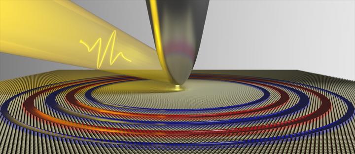
The Illustration above shows plasmon waves created by an ultrafast laser coupled to an atomic force microscopy tip. The plasmon waves are shown as concentric red and blue rings moving slowly across an atomically thin layer of TaS2.


