

Monolithically integrated GaN power ICs
The demonstration of half-bridges and single-stage buck converters takes GaN power ICs another step forward
BY XIANGDONG LI AND STEFAAN DECOUTERE FROM IMEC
OVER THE LAST FEW YEARS discrete GaN HEMTs have been taking an increasing share of the power electronics market. Thanks to their fundamental superiorities over their silicon rivals. Merits of these wide bandgap transistors include a lower on-resistance, smaller parasitic capacitance and a higher critical electrical field. In addition, GaN HEMTs switch at higher frequencies, enabling power systems based on this technology to be smaller and lighter, due to a reduction in the size of passive components. Yet another attribute of these devices is their reverse conduction capability, accomplished without the need for the low-performance body diode, which is detrimental when deployed in a typical silicon VDMOS power device.
For fail-safe operation, enhancement-mode (E-mode) p-GaN gate HEMTs have been widely accepted by various vendors, and used for a wide variety of applications that range from AC-DC converters and DC-DC converters to bridgeless totem pole power-factor correction circuits and class D Audio amplifiers.
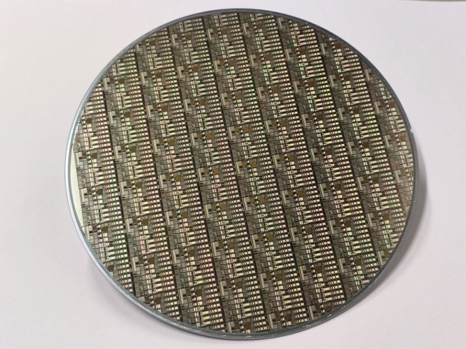
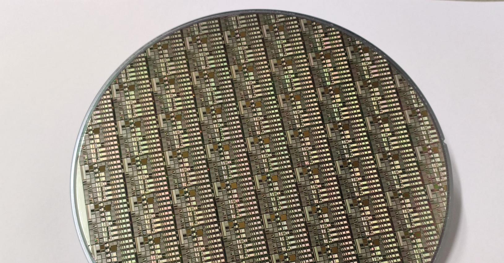
Figure 1. Processed GaN ICs on a 200 mm GaN-on-SOI substrate.
To build on all this success, the next step is the development of a GaN integrated power IC. Such a circuit promises to enhance the potential for fast-switching GaN power HEMTs by suppressing parasitic inductance and trimming the size of the chip.Various building blocks are needed for the production of all-GaN power ICs. These modules include: half-bridges, diodes, capacitors, drivers, dead-time control, level shifters, pulse-width modulation, diagnostic and protection circuits, regulators, a bandgap reference, and bootstrap circuits.Much effort has been devoted to integrating these single or multiple modules on GaN-on-silicon. Progress is not easy. One major obstacle is that all-GaN ICs on traditional silicon substrates are hampered by a lack of effective isolation – this induces a back-gating effect in the half-bridge. A second stumbling block is the absence of a complementary GaN pFET, which is a bottleneck for integrating high-performance logic circuits and inverting amplifier stages.
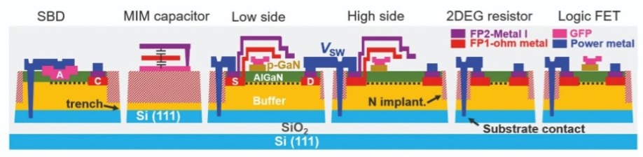
Figure 2. GaN IC components on a GaN-on-SOI substrate.
At imec of Leuven, Belgium, we have been developing a GaN IC technology that addresses both these issues. We realise electrical isolation between different modules and components by combining trench isolation with the incorporation of a buried oxide layer on a silicon-on-insulator (SOI) substrate. Adopting this approach supresses crosstalk between various components and enables the separate substrate of each device to be decoupled, because the silicon(111) top layer in the SOI is fully cut-off by deep trench isolation. With our design, the local substrate contact provides an electrical connection between the source and the substrate, thus ensuring an equal potential between them. This feature is highly valued, as it avoids any back-gating effect. We tackle the second issue, the absence of the GaN pFET, by using a single-transistor inverter with a resistive load to provide an inverting function.We have already demonstrated the feasibility of our technology for developing functional GaN HEMTs and related components that are key to an integrated all-GaN power IC. This breakthrough has involved activity in many areas, from epitaxy to integration, modelling and simulation. The result is a technology that has proved its worth by the functionality of our GaN power ICs.
Epitaxy and integration
Our team has developed GaN power IC integration technology on 200 mm GaN-on-SOI wafers with very little warp and a high degree of uniformity (see Figure 1). We begin with a 1070 μm-thick silicon (111) handling wafer that contains a 1.5 μm-thick SiO2 buried layer and a 1.5 μm-thick silicon (111) top layer. We load this engineered wafer into an MOCVD reactor and add a 200 nm-thick AlN nucleation layer, followed by a 3.25 μm (Al)GaN buffer layer, a 400 nm GaN channel layer, a 12.5 nm Al0.23Ga0.77N barrier layer and an 80 nm magnesium-doped p-GaN layer with a doping concentration of about 3×1019 cm-3. The stepped superlattice buffer, specifically designed by our team, controls the stress during epitaxy. Thanks to this, we avoid excessive wafer warp.
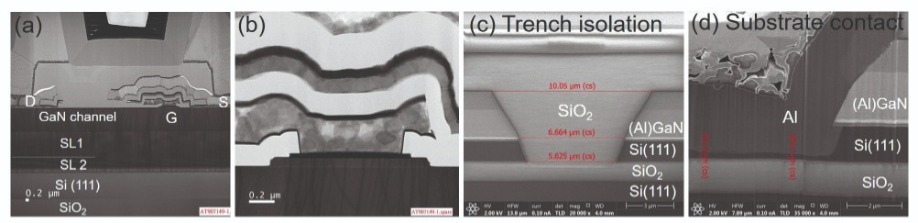
Figure 3. Cross-sectional transmission electron microscopy images of the (a) 200 V p-GaN gate HEMT, buffer stack, and substrate, and (b) detailed gate module, and focused ion beam, scanning electron microscopy images of the (c) 6 μm-wide trench isolation and (d) substrate contact.
We process these epiwafers, using nitrogen implantation to provide horizontal isolation. The back-end power metal aluminium ensures substrate contact and interconnection. Using this approach, we can produce a range of modules (examples are provided in Figure 2). We have scrutinised some of these structures with different forms of electron microscopy (see Figures 3(a) and (b) for transmission electron microscopy images of the p-GaN gate power HEMT and gate module, respectively; and Figures 3(c) and (d) for scanning electron microscopy images for evaluating trench isolation and the substrate contact).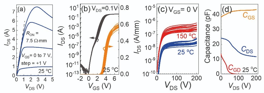
Figure 4. (a) Output, (b) transfer, (c) off-state leakage, and (d) C-V characteristics of the fabricated 40 mm p-GaN gate power HEMT on the 200 mm GaN-on-SOI substrate. The device shows a low Ron of just 7.5 Ω mm, a uniform high Vth of more than 3 V, and an off-state leakage of less than 1 µA/mm.
Measurements on our 40 mm p-GaN gate power HEMT produce promising results. On-resistance is just 7.5 Ω mm; there is a uniform, high threshold voltage – it is over 3 V; and off-state leakage is below 1 μA/mm (see Figure 4 for details). This low on-resistance, combined with low parasitic capacitance, guarantees a low loss during operation, while the high threshold voltage ensures that devices are resistive to faulty turn-on, which stems from the Miller current during high-voltage switching.Evaluating modules
One significant weakness of conventional GaN-on-silicon HEMTs is that their low side and high side share the same common conductive silicon (111) substrate, which is normally grounded. Due to this, when the high side is switched on, the drain current is jeopardized dramatically by the negative substrate-to-channel potential difference. In contrast, with our approach, this potential difference is fixed at zero, thanks to the local substrate contact and deep trench isolation. This architecture guarantees a very stable high-side drain current, and ultimately eliminates the back-gating effect, paving the way to GaN power ICs.
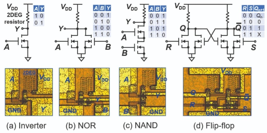
Figure 5. Schematic, truth table, and photograph of (a) inverter, (b) NOR gate, (c) NAND gate, and (d) flip-flop, designed in resistor-transistor logic.
For large-scale logic, key ingredients are the inverter, NOR gate, NAND gate and flip-flop. We use resistor-transistor logic to build these functions. This involves replacing the pMOS with a 5 μm-wide meander two-dimensional electron gas resistor, and using a p-GaN gate HEMT with a 6 μm gate width and a 1.5 μm gate-to-drain spacing for the logic nFET (see Figure 5).After packaging these fabricated blocks, we evaluated them with switching tests. The results are encouraging, with waveforms that exactly follow the truth tables (see Figure 6). Thanks to this success, we have been able to construct more complex ICs in power systems, such as diagnostic and protection circuits, based on these fundamental blocks.
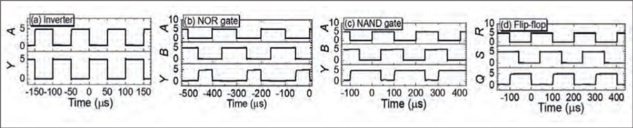
Figure 6. Measured switching waveforms of the (a) inverter, (b) NOR gate, (c) NAND gate and (d) flip-flop.
To drive our HEMTs, we use an integrated two-stage driver. It has an inverter as the first stage and a push-pull driver as the second stage is (see Figures 7(a) and (b)). To evaluate this IC, we use a PCB for double pulse tests ((Figure 7(c)). Using these tests, we have evaluated the switching waveforms and current handling capability of the HEMT with its integrated driver – the results are shown in Figure 7 (d). Rise and fall times are both around just 10 ns, and could be even shorter by improving the PCB design and the test set-up.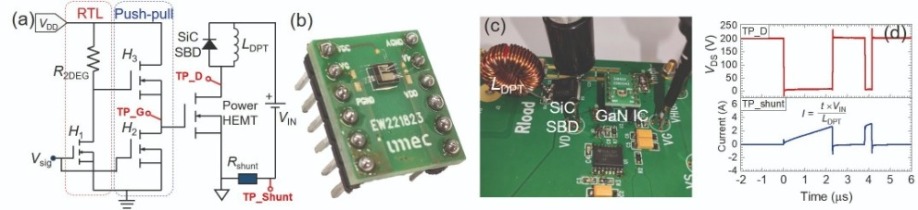
Figure 7. (a) The double pulse test (DPT) circuit, (b) packaging of the GaN IC with an integrated driver and power HEMT, (c) printed circuit board (PCB), and (d) DPT switching waveforms and current handling capability of the HEMT with integrated driver.
We have also built a GaN IC with an asymmetric half-bridge and integrated drivers, and connected this to a PCB test board (see Figure 8). Testing reveals swift and stable switching waveforms (see Figure 9). This proves that we have thoroughly overcome the back-gating effect, which bottlenecks half-bridge integration.By connecting the output stage, we can configure this IC as a 48 V-to-1 V single-stage buck converter. After a settling time of tens of microseconds, the output voltage is gradually stabilized at 1 V (see Figure 10(a)). A single pulse has a width of just 46 ns (see Figure 10(b)).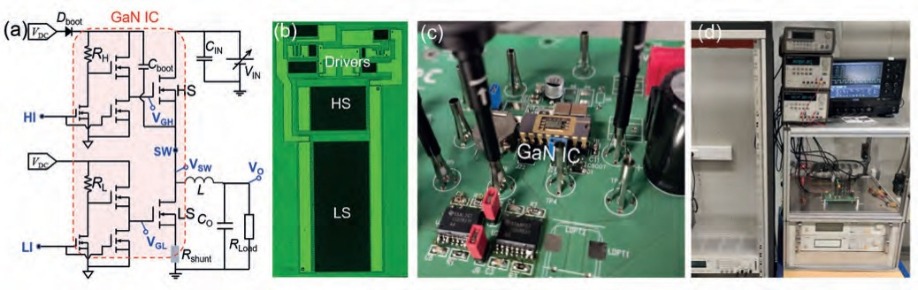
Figure 8. (a) imec’s GaN IC with integrated half-bridge and drivers for use in a buck converter, (b) photograph of the fabricated half-bridge with integrated drivers, (c) test board, and (d) test setup.
All-GaN power ICsFor the GaN IC design, we modified MIT virtual source GaN HEMT models for E-mode p-GaN gate HEMTs and used spice models for the resistors. We have designed a monolithically integrated all-GaN buck converter using our 200 V GaN IC platform process design kit, which includes process documentation, library devices, layout guidelines for custom design, verification and models (see Figure 11).
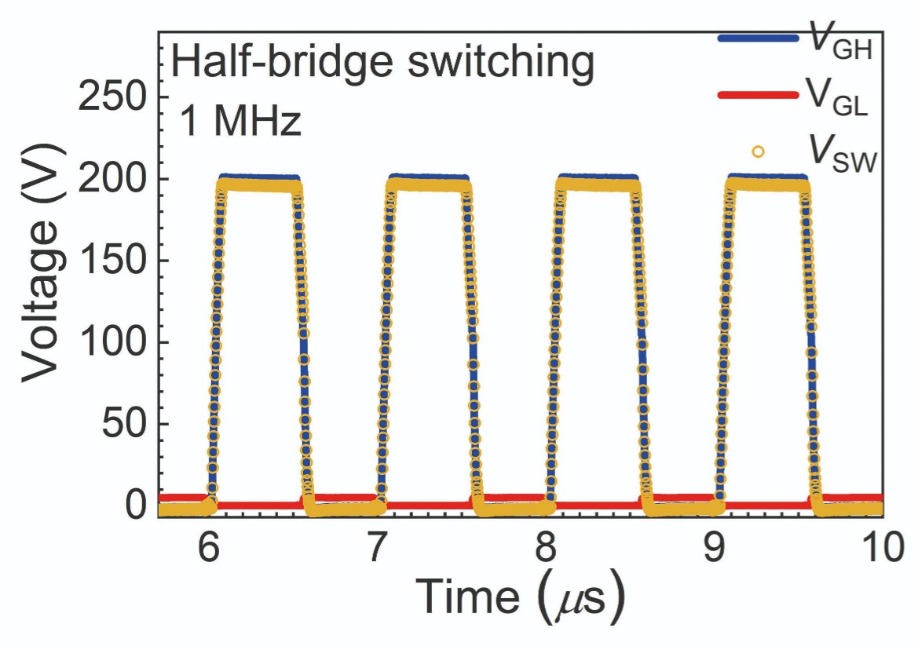
Figure 9. The 200 V half-bridge switching test is first executed on the test board by disconnecting the output stage of L, CO, and Rload. Two 1 MHz non-overlapping signals, HI and LI, with a dead time of 40 ns, are sent to the two driver input terminals and the waveforms of VGH, VGL, and VSW are monitored. Previous studies show distortion of switching waveforms, due to the back-gating effect in a half-bridge on GaN-on-silicon without substrate isolation. In this case, the back-gating effect is fully mitigated thanks to the trench isolation.
In this GaN IC a crucial role is played by the module that provides pulse-width modulation. It consists of a ramp generator and an error amplifier, each having a comparator designed in resistor-transistor logic. The voltage is directly converted from 48 V to 1 V by this all-GaN power IC, an approach that is far simpler than a silicon-based multiple-stage converter (see Figure 11(b)).This GaN IC is a major milestone in the advancement of this technology, as it is the first step towards a real smart power IC based on p-GaN technology. Note that the designed all-GaN ICs have been successfully processed on 200 mm GaN-on-SOI (see Figure 11(c)).
Given that this work is still in its infancy, it is not surprising that there is still room to improve the performance of our GaN ICs. We have noticed that the resistor-transistor logic is impaired by high static power dissipation and a long RC delay, which are problematic for some high-speed analogue ICs. But the good news is that we are developing new integration technology. This includes integrating a depletion-mode HEMT, which replaces the two-dimensional electron gas with E/D-mode co-integration and will drive an improvement in GaN IC performance.
Another challenge that we face is unifying the epitaxy and processing for different components. For instance, E-mode p-GaN gate HEMTs require p-GaN epitaxy – but this inevitably contaminates D-mode HEMTs. In addition, we need to learn how to unify different passivation strategies. We are interested in initial studies on GaN pFETs reported by other groups, but the approaches that have been pursued are a long way away from being applicable.
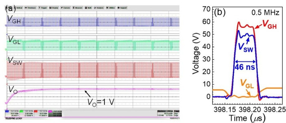
Figure 10. Transient switching waveforms of the 48 V-to-1 V single-stage buck converter, where the VO gradually stabilised at 1 V, proving the function of the GaN IC, (b) detailed single pulse of the converter, highlighting a narrow pulse width of 46 ns and a low duty cycle of 2.2 percent, which guarantees the high switching frequency of 0.5 MHz
An alternative, pioneered by Intel, is three dimensional integration (see Stacking GaN and silicon transistors on 300 mm silicon). That involves processing E-mode GaN NMOS on the underneath of a GaN-on-silicon wafer, and building silicon PMOS transistors on the top silicon layer by a layer transfer process.One tremendous opportunity for GaN power ICs is the co-integration of GaN Schottky barrier diodes. Their silicon cousins cannot sustain voltages of more than 200 V. Due to this restriction, the rectifying circuits, power factor correction circuits, and switch mode power supplies that operate at more than 200 V often employ silicon diodes with a p-n junction. That’s not ideal, as the resulting circuits suffer from a high reverse-recovery charge, leading to a high switching loss.
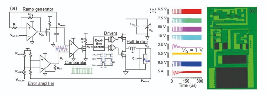
Figure 11. Design of a monolithically integrated all-GaN buck converter comprising half-bridge, drivers, dead-time control, comparator, error amplifier, and ramp generator, (b) simulation waveforms by Cadence based on imec device models and PDK (process design kit), and (c) processed circuit.
Replacing these diodes with those made from GaN offers a big step forward, as they combine higher blocking voltages with reduced switching loss. Ideally, this is accomplished by co-integrating the GaN Schottky barrier diodes with the GaN half-bridge circuitry, as this further simplifies power system design. It is important to connect the anode of these diodes to the silicon (111) layer, as this suppresses the impact of buffer trapping on forward conduction. Crosstalk between the half-bridge and the diodes is efficiently decoupled by trench isolation, together with the buried oxide of the GaN-on-SOI technology. We are left in no doubt that GaN-on-SOI is a promising platform for GaN power ICs, based on our comprehensive investigation that began with considerations for the substrate and buffer and went on to consider the isolation to the device, co-integration, and circuit design. Our efforts have enabled different components to be successfully co-integrated on this platform. This is highlighted by the performance of our demonstrator 200 V half-bridge and 48 V-to-1 V single-stage buck converter GaN ICs.- This technology is accessible through the EUROPRACTICE prototyping service.
X. Li et al. GaN-on-SOI: Monolithically Integrated All-GaN ICs for Power Conversion. in IEDM Tech. Dig., pp.4.4.1-4.4.4, Dec. 2019
X. Li et al. IEEE Electron Dev. Lett. 40 1499 (2019)
X. Li et al. IEEE Electron Dev. Lett. 39 999 (2018)
S. You et al., “Monolithically integrated GaN power ICs designed using the MIT virtual source GaNFET (MVSG) compact model for enhancement-mode p-GaN gate power HEMTs, logic transistors and resistors”, pp. 158-161, ESSDERC 2019
GaN-IC Technology, http://europractice-ic.com/mpw-prototyping/power-electronics


