Loading...
News Article

JH opens Analytical Lab Services

News

New services company will provide complete outsourced process solutions to support customers with their medical device, semiconductor, metallography and other applications

JH Technologies, a distributor of optical and digital imaging systems, materials preparation, testing and analysis systems, and metrology tools announces that it recently opened JH Analytical Lab Services at the company’s headquarters in Fremont, California.

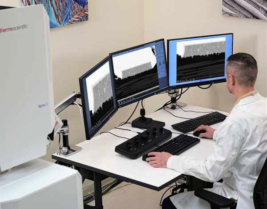
JH Analytical Lab Services will provide complete outsourced process solutions to support customers with their medical device, semiconductor, metallography and other applications. The analytical laboratory services include: Sample preparation and analysis, cross sections, metallurgical analysis and hardness testing, SEM/EDS, 2D/3D X-ray, and process improvement.

“We are excited to bring these analytical lab services to our customers,” said JH Technologies CEO John Hubacz. “We started this venture based on customer requests asking for our expertise to help them solve their most challenging problems. Our goal is to provide world class service to all customers, from the smallest start up to well established manufacturers”.

JH Analytical Lab Services will operate under the direction of general manager Micah Harrel, who has been with JH Technologies for nearly 30 years. Lab director Jerome Pons joined the company in 2018 and brings customers more than 20 years of experience in sample preparation and electron microscopy, including developing new techniques to improve efficiency and perform high quality sample preparation.

In addition to being supported by decades of experience, the JH lab is equipped with the latest in analytical equipment including scanning electron and optical microscopes, tools for EM sample preparation, hardness testing and more.

SiC MOSFETs: Understanding the benefits of plasma nitridation
Wolfspeed reports Q2 results
VueReal secures $40.5m to scale MicroSolid printing
Mitsubishi joins Horizon Europe's FLAGCHIP project
Vishay launches new high voltage SiC diodes
UK team leads diamond-FET breakthrough
GaN adoption at tipping point, says Infineon
BluGlass files tuneable GaN laser patents
QD company Quantum Science expands into new facility
Innoscience files lawsuit against Infineon
Riber revenues up 5% to €41.2m
Forvia Hella to use CoolSiC for next generation charging
Photon Design to exhibit QD simulation tool
Ortel transfers CW laser fabrication to Canada
Luminus adds red and blue multi-mode Lasers
PseudolithIC raises $6M for heterogeneous chiplet tech
Mesa sidewall design improves HV DUV LEDs
IQE revenue to exceed expectations
'Game-changing' VCSEL system targets clinical imaging
German start-up secures finance for SiC processing tech
Macom signs preliminaries for CHIPS Act funding
IQE and Quintessent partner on QD lasers for AI
EU funds perovskite tandems for fuel-free space propulsion
EU to invest €3m in GeSi quantum project
Transforming the current density of AlN Schottky barrier diodes
Turbocharging the GaN MOSFET with a HfO₂ gate
Wolfspeed launches Gen 4 SiC MOSFET technology
Report predicts high growth for UK's North East
Element Six unveils Cu-diamond composite
SemiQ launches hi-rel 1700V SiC MOSFETs
Lynred to exhibit Eyesential SWIR sensor for machine vision
Thorlabs buys VCSEL firm Praevium Research
×
Search the news archive

To close this popup you can press escape or click the close icon.
Logo
x
Logo
×
Register - Step 1

You may choose to subscribe to the Compound Semiconductor Magazine, the Compound Semiconductor Newsletter, or both. You may also request additional information if required, before submitting your application.


Please subscribe me to:


You chose the industry type of "Other"

Please enter the industry that you work in: