
2D transistor has brain-like energy efficiency
Swiss team uses WSe2 and SnSe2 to make a tunnelling transistor that is almost as energy-efficient as the human brain
Researchers at the EPFL (École Polytechnique Fédérale de Lausanne) Nanoelectronic Devices Laboratory, working under Adrian Ionescu, have designed and demonstrated a new type of technology based on 2D semiconducting materials that’s almost as energy-efficient as the human brain.
Smartphones, laptops and smartwatches consume vast quantities of energy, yet only around half of this energy is actually used to power important functions. With billions of these devices in use worldwide, a significant amount of energy goes to waste. Adrian Ionescu and his team at EPFL’s Nanolab have launched a series of research projects in the quest to make transistors more energy-efficient.
“The transistor is the most abundant artificial object ever created by humans,” says Ionescu. “It enables our entire computational infrastructure and the way we interact in real time with portable information processing in the 21st century. It forms the basic building block for both digital and analog signal processing.”
Energy efficiency matters
“Today, we know that the human brain consumes about the same quantity of energy as a 20 Watt bulb,” says Ionescu. “Despite consuming so little energy, our brain is capable of performing tasks that are several orders of magnitude more complex than what a computer can handle – analysing information provided by our senses and generating intelligent decision-making processes. Our goal is to design electronic technology for portable devices that’s similar in efficiency to human neurons.”
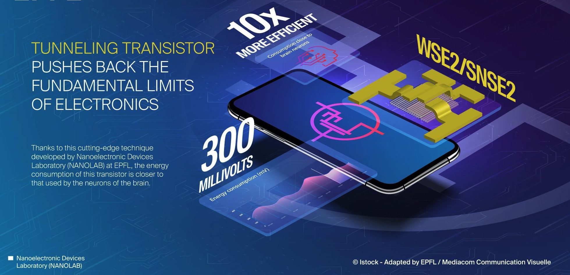
The transistor built by the EPFL researchers raises the bar for energy efficiency. Developed in the School of Engineering (STI) clean room, it comprises 2D layers of WSe2 and SnSe2. Known as a 2D/2D tunnelling transistor, it exploits the band alignment of the WSe2/SnSe2 gate junction. And because it measures just a few nanometers, it is invisible to the human eye. As part of the same research project, the Nanolab team also designed a new hybrid dual-transport structure that could one day push technology performance even further.
Breaking limits
With this transistor, the EPFL team has also broken one of the fundamental limits of electronic devices. “Think of a transistor like a switch that requires energy to turn on and off,” explains Ionescu. “By analogy, imagine how much energy it would take to climb to the top of a Swiss mountain and descend down into the next valley. Then think how much energy we could save by tunnelling through the mountain instead.
"This is exactly what our 2D/2D tunnel transistor achieves: it performs the same digital function using much less energy.” Until now, scientists and engineers had failed to break this fundamental energy-consumption limit for 2D/2D components of this type. But the new transistor changes all that, setting a new standard for energy efficiency in the digital switching process. The Nanolab team worked with the group led by Mathieu Luisier at ETH Zurich to test and confirm the new tunnel transistor’s properties via atomistic simulation. “This is the first time that we’ve broken through this fundamental limit, while at the same time achieving higher performance than a standard transistor made from the same 2D semiconducting material, and at a very low voltage supply,” says Ionescu.
From wearables to edge AI
This new technology could be used to build electronic systems that are almost as energy-efficient as the neurons in our brain. “Our neurons operate at around 100 millivolts (mV), or roughly 10 times less than the voltage supplied by a standard battery,” says Ionescu. “Our technology currently operates at 300 mV, making it around 10 times more efficient than a conventional transistor.” No other electronic component in existence today comes close to this level of efficiency.
This breakthrough has potential applications in two areas: wearable technologies (such as smartwatches and smart clothing) and chips for edge AI. But turning this lab proof-of-concept into an industrial product will still require several more years of hard work
'WSe2/SnSe2 vdW heterojunction Tunnel FET with subthermionic characteristic and MOSFET co-integrated on same WSe2 flake' by Nicolò Oliva et al; Npj 2D Materials and Applications 4, Article 5 (2020).


