
Membranes light up silicon photonics

Epitaxial growth on wafer-bonded InP templates enables the integration of high-performance lasers and
Mach-Zehnder modulators with silicon waveguides.
By Tatsurou Hiraki, Takuma Aihara, Takuro Fujii, Koji Takeda, Takaaki Kakitsuka, Tai Tsuchizawa and Shinji Matsuo From NTT Corporation
The outbreak of Covid-19 has lead to more teleworking, more steaming of films and more on-line gaming. All of this is driving up global Internet traffic, which had already been growing at an exponential rate for many years. To address this demand, more data centres are being deployed. This solves one problem, but adds to another – humanity’s carbon footprint. To prevent the carbon emissions from this sector escalating to a level where it accounts for a significant fraction of the world’s energy consumption, data centres need to be built with components that draw very little power. To win sales, these products must also be competitively priced and compact, so that they can help to minimise the size of this infrastructure.
A key component in every data centre is the optical transceiver. To increase transmission capacity, it must incorporate Mach-Zehnder modulators, as they enable high baud rates and signals for advanced modulation formats.
One promising technology for meeting these requirements is silicon photonics. It slashes the cost and size of photonic integrated circuits (PICs) by providing ultra-compact waveguide circuits on large, inexpensive silicon wafers. And it has yet another merit: it is compatible with CMOS fabrication technology, an attribute that opens the door to monolithic integration of silicon-based Mach-Zehnder modulators, compact waveguide filters, spot-size converters for fibre coupling, polarization rotators and splitters, and germanium photodetectors on silicon-on-insulator wafers. Today, several companies are drawing on silicon photonics for the design and commercialisation of optical transceivers.
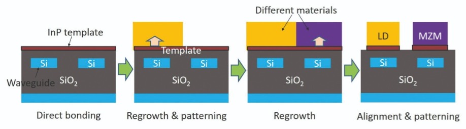
Figure 1. Procedure for integrating III-V semiconductor devices with different bandgaps by direct bonding and epitaxial growth.
However, there is a critical problem with the silicon-based optical transceiver: it lacks a monolithically integrated laser diode, due to the indirect bandgap of silicon. Due to this, an external laser diode must be attached to the optical transceiver, increasing size and cost.There is also another issue with the silicon-based Mach-Zehnder modulator. It has a poor modulation efficiency, because silicon is only able to exploit the inefficient carrier-plasma effect. For this class of modulator, a key figure of merit, known as the half-wave-voltage-length product (VπL), is typically larger than 1 V cm. This high value hampers efforts to trim the size and the power consumption of silicon-based optical transceivers.
An attractive solution to these issues is to heterogeneously integrate III-V semiconductors on a silicon platform. A good choice for this is the InP-based family of materials, which is an established, mature technology for making lasers for telecommunication applications. Another attribute of InP-based materials is that they have a much larger refractive-index change than silicon, thanks to their strong carrier-plasma, band-filling, and Franz-Keldysh effects. These phenomena assist the fabrication of high-efficiency phase shifters for Mach-Zehnder modulators with a small VπL.
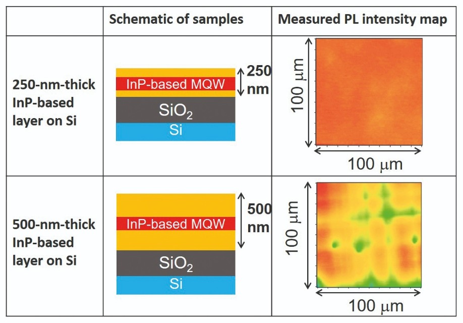
Figure 2. Measured photoluminescence intensity distributions of InP-based layers bonded onto SiO2/silicon substrates and annealed at 610 °C for 30 minutes.
To produce transceivers with this technology requires the integration of laser diodes and Mach-Zehnder modulators with a silicon platform. One way to do this is to bond different devices to a silicon waveguide circuit. With this approach, the laser diode and Mach-Zehnder modulators are fabricated on different III-V semiconductor wafers, before each is bonded to a silicon waveguide circuit, using precise alignment. A downside of this approach is that it is challenging to realise the high throughput needed to integrate a large number of components. Alternatively, monolithic integration can be realised through epitaxial growth of different III-Vs on silicon. This has the potential to provide low-cost, wafer-level integration, as lithography techniques allow patterning and aligning of all devices. But success is not assured, because it is difficult to obtain high-quality layers of crystalline III-Vs, due to their lattice mismatch with silicon. So, whatever approach is adopted, it is far from easy to integrate simultaneously laser diodes and Mach-Zehnder III-V modulators on a silicon platform.A hybrid solution
At the NTT Device Technology Labs in Kanagawa, Japan, our team is developing a novel fabrication method that addresses these issues. Our technology combines direct bonding and epitaxial growth to integrate various III-V devices with different bandgaps on silicon waveguide circuits (see Figure 1).
Fabrication begins by bonding a III-V template to a SOI wafer, and then re-growing different materials on the lattice-matched template, which could be a thin film of InP on SiO2/silicon. Our next step is to use lithographic processes to align and pattern all the III-V devices on the silicon waveguide circuits. With this approach, as well as using epitaxial growth on the lattice-matched template, we can integrate a variety of high-quality materials with different bandgaps. It is this high degree of flexibility that allows us to integrate many high-performance III-V devices.
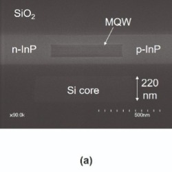
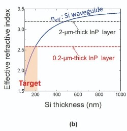
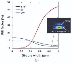
Figure 3. (a) Cross-sectional, scanning-electron microscopy of a membrane laser diode. (b) Calculated effective refractive index of silicon waveguides and InP layers. (c) Calculated fill factors in the multi-quantum well, p-type InP, and silicon cores. The area of the multi-quantum well core is set to 0.6 x 0.1 µm2.
When applying this technique, we had to consider the critical thickness of the epitaxial layers on the bonded template. This thickness is determined by the difference between the thermal expansion coefficient of the bonded III-V layer and the silicon substrate. For example, for the epitaxial growth of an InP layer on a silicon substrate at 600 °C, the critical thickness is 430 nm. That is concerning, since the typical thickness of both a conventional semiconductor laser diode and a Mach-Zehnder III-V modulator are 2 µm to 3 µm. As these devices are much thicker than the critical thickness, it makes it very difficult to integrate conventional III-V semiconductor devices on a silicon platform with an epitaxial growth process.Membrane devices
Our solution is to trim the thickness of the III-V layers, as this reduce thermal strain during the epitaxial growth process. The success of this approach is illustrated in measurements of photoluminescence intensity (see Figure 2). They reveal that there is very little strain in the InP-based layers that are bonded to SiO2/silicon substrates, prior to annealing for 30 minutes in an MOCVD chamber, using the following conditions: 610°C, a PH3 atmosphere and a pressure of 30 Torr. While photoluminescence measurements on structures with 500 nm-thick InP-based layers that include 150 nm-thick multi-quantum-well layers have dark lines, due to exceeding the critical thickness, those that are 250 nm-thick and feature an identical active region are free from degradation, due to the lower thermal strain. These results highlight the necessity of using a membrane structure for epitaxial growth on the silicon substrate.
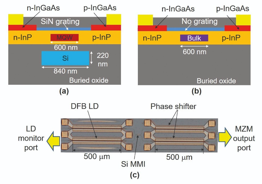
Figure 4. Cross sections of (a) laser diode and (b) phase shifter. (c) Microscopy image of a fabricated laser diode and Mach-Zehnder modulator device.
Based on these findings, we have developed membrane buried-heterostructure lateral p-i-n and p-n diodes for lasers, optical amplifiers, and Mach-Zehnder modulators on a silicon platform. Note that the buried heterostructure is a valuable feature, enabling efficient confinement of both carriers and photons. To integrate the various lateral diode devices, we use silicon ion implantation and zinc thermal diffusion processes to form the donor and acceptor regions, respectively. Using these techniques, we define donor and acceptor regions with photolithography processes, and thus obtain different carrier profiles for the laser diode and the Mach-Zehnder modulator. This is critical to integrating laser diodes and Mach-Zehnder modulators on a silicon platform.Using this method, we have fabricated a lateral-current-injection p-i-n diode for the laser diode (see Figure 3(a)). At its heart is a multi-quantum-well core, buried in the 230 nm-thick InP layer and precisely aligned to the silicon waveguide core. This membrane buried heterostructure overcomes another issue facing typical InP-based vertical diodes on a silicon platform – it provides effective refractive-index matching between the III-V and silicon layers.
For optical coupling between the InP and silicon layer, calculations indicate that a typical vertical diode requires a silicon-waveguide layer with a thickness between 400 nm and 500 nm. However, the silicon waveguides widely developed for low-loss and compact channel-waveguide circuits have a thickness of only 220 nm (see Figure 3(b)). In other words, a typical vertical InP-based device is not compatible with these thin silicon waveguide circuits. Fortunately, that’s not the case for our membrane InP-based layer, which is much thinner than the conventional 2 µm-thick InP layer, and comparable to that of the widely used 220 nm-thick silicon waveguide layers. This means that thanks to effective index matching, it is easy to couple our InP-based membrane devices to mature silicon waveguide circuits.
Efficient optical coupling between the multi-quantum well core and low-loss silicon waveguide holds the key to reducing the internal optical loss of the laser diode. Calculations of fill factors in the multi-quantum well core, p-type InP, and silicon cores indicate that thanks to index matching, we can control the fill factors by changing the width of the silicon core (see Figure 3(c)). As a result, overlap with the large-loss, p-type InP region can be reduced by increasing the overlap with the low-loss 220 nm-thick silicon core. Making good use of this, we set the silicon core width to 840 nm to provide a fill factor of around 4 percent in the multi-quantum well. We can change the fill factors of our membrane structure while maintaining the small multi-quantum-well area, enabling us to reduce the threshold current. The upshot of all of this flexibility is that by using the membrane structure, we can obtain high-performance laser diodes on widely developed, 220 nm-thick silicon waveguide circuits.
Integrating laser diodes and modulators
Drawing on the insights provided by our calculations, we have integrated a membrane laser diode with an InP-based Mach-Zehnder modulator on a silicon platform (cross-sections of our membrane laser diode and phase shifter for the Mach-Zehnder modulator are shown in Figures 4(a) and 4(b), respectively). For this particular design, we use a 500 µm-long distributed-feedback laser with a SiN grating on the top of the InP layer. To ensure operation in the C-band, we set the photoluminescence peak wavelengths for the multi-quantum-well core of the laser diode to 1.52 µm, and that for the n-type InGaAsP-bulk core of the phase shifter to 1.3 µm. As both the laser diode and phase shifter are formed in 230 nm-thick InP-based layers, they can be integrated using the epitaxial growth process on a silicon platform.

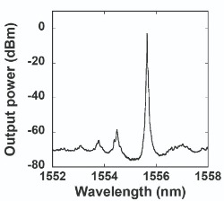

Figure 5. (a) Measured light-output curve from the laser diode port of the laser. The chip facet faced air in this experiment, creating a power fluctuation, due to optical reflection at the facet. (b) Measured output spectrum from the modulator, using a laser diode current of 50 mA and a Mach-Zehnder modulator DC voltage of 4.5 V. A refractive-index-matching oil is inserted between the high-numerical-aperture fibre and the silica core to reduce the reflection at the chip facet. (c) Measured eye diagram for NRZ 28 Gbit/s signal.
We designed the phase shifter for a high-efficiency, carrier-depletion, Mach-Zehnder modulator. As shown in Figure 4(b), the buried InGaAsP-bulk core of the phase shifter does not couple to the silicon waveguide. With this design, there is a large fill factor of around 30 percent in the n-type InGaAsP core – it exceeds the values associated with conventional III-V semiconductor phase shifters with thicknesses of 1 µm to 2 µm. By applying reverse bias to the n-type InGaAsP core, we can efficiently modulate the optical phase using a combination of the carrier-plasma effect, the band-filling effect, and the Franz-Keldysh effect. This type of membrane phase shifter has a typical VπL of around 0.4 V cm, a figure far lower than that for a typical silicon carrier-depletion Mach-Zehnder modulator, which has a VπL higher than 1 V cm. Another attribute of the membrane structure is its low capacitance, which is useful for reducing the capacitance-resistance time constant of the phase shifter.Building on this success we have united components, with a 500 µm-long DFB laser diode integrated on the silicon waveguide and connected to the Mach-Zehnder modulator (see the microscopy image, shown in Figure 4(c)). The modulator has silicon multimode interferometers and 500 µm-long membrane phase shifters. At the chip facet there is a silica-based (SiOx) core with an area of 3 x 3 µm2, designed for low-loss fibre coupling. The role of the narrow inverse silicon taper is to convert the optical mode field diameter from the nanowire silicon waveguide to the SiOx waveguide. The SiOx core provides easy butt-coupling to the optical fibre, realising low loss and low reflection.
Our narrow inverse InP tapers are designed to transfer the optical mode fields between the laser diode or phase shifter and the single-mode silicon waveguide. The inverse taper, 50 µm in length and with a cross-sectional area of 0.1 x 0.23 µm2, launches light into the single-mode silicon waveguide that has a cross-sectional area of 0.44 x 0.22 µm2. As the aspect ratio of the taper tip is much lower than that of conventional InP devices, it is relatively easy to fabricate this narrow membrane taper using a mature process. Using this mode converter, we integrate the membrane laser diode and phase shifters with silicon waveguides, realised with low loss and low reflection.
To realise wafer-level integration of both laser diodes and Mach-Zehnder modulators on a silicon platform, we pattern silicon waveguides on a SOI wafer, before burying them in a SiO2 cladding film. Chemical-mechanical polishing of this cladding flattens its surface and reduces its thickness on the silicon waveguide to 100 nm. After this, we remove the InP substrate. The whole multi-quantum well layer is taken away, except for the laser diode region, to leave a 50 nm-thick InP template on the entire wafer. An n-type InGaAsP-bulk layer is then regrown for the phase shifter, before the cores for the laser diode and phase shifter are patterned by lithography. The next steps are: the re-growth of an InP layer to form a buried heterostructure; re-growth of an InGaAs contact layer; and patterning donor and acceptor regions by lithography, followed by their formation with silicon ion implantation and zinc thermal diffusion. The latter step enables us to obtain different carrier profiles for the laser diode and phase shifter on the entire wafer. Completion of the fabrication process involves patterning the InGaAs contact layer and InP mesa and tapers, before turning to a backend process, used to add electrodes and produce a large silica-based core for fibre coupling. By forming the large silica core at a temperature below 200 °C, we avoid damage to the III-V devices.
Proven success
Measurements of output power from the laser diode port, made with a photodetector directly facing a chip facet that detects the total output power coming from it, reveal that the threshold current is only 4.5 mA (see Figure 5(a)). This low value, given the 500 µm active length of the laser diode, is attributed to the small active area. Increasing the injection current to 70 mA propels the output power to around 5.5 mW. This figure indicates that we prevented fatal damage to the active layer during the regrowth processes, and highlights that the membrane InP-based layer is beneficial for reducing thermal strain during the epitaxial growth process.
To evaluate the output power from the Mach-Zehnder modulator’s output port, we aligned a high-numerical-aperture fibre with the silica core at the chip facet. The fibre-coupled output power hits 2.9 mW when driving the laser diode at 70 mA, with tuning of the DC bias of the phase shifter maximising the output power from the measured port. We attribute this high output power to efficient light emission from the membrane laser and to low losses of the Mach-Zehnder modulator and spot-size converter.
Additional measurements reveal that the half-wave voltage (Vp) of the Mach-Zehnder modulator is around 7.5 V. It follows that VpL is around 0.4 V cm, a value more than three times smaller than that of a typical silicon carrier-depletion Mach-Zehnder modulator. These results show that we have succeeded in integrating a high-efficiency InP-based Mach-Zehnder modulator on a silicon platform.
We have also demonstrated dynamic modulation of our laser diode and Mach-Zehnder modulator integrated device. Using a DC bias of 4.5 V for the Mach-Zehnder modulator, to ensure modulation of non-return-to-zero signals, we have investigated the output spectrum at different drive currents for the laser diode. These measurements, made without an RF input to the phase shifter, show single-mode lasing with a side-mode suppression ratio of around 55 dB, for a drive current of 50 mA (see Figure 5(b)).
To evaluate the modulation capability of our design, we have applied RF input signals from a pulse pattern generator to one of the phase shifters in the Mach-Zehnder modulator. This produced a clear eye opening using the following conditions: a laser diode current of 42 mA; a non-return-to-zero 28-Gbit/s signal; without 50 Ω termination at the Mach-Zehnder modulator.
Our next goal is to use our technology to integrate narrow-linewidth laser diodes and in-phase and quadrature modulators for optical transceivers in telecommunication systems. Further ahead, the uses of our platform will expand, as it is not limited to integrating laser diodes and Mach-Zehnder modulators, but can be used to construct other III-V devices with different bandgaps on a silicon platform. This virtue makes our technology ideal for constructing low-cost, large-scale, high-performance PICs with high functionality for various applications.
T. Hiraki et al. “Integrated DFB Laser Diode and High-efficiency Mach-Zehnder Modulator using Membrane III-V Semiconductors on Si Photonics Platform,” 2019 IEEE International Electron Devices Meeting (IEDM), San Francisco, U.S.A, 33.4 (2019)
T. Fujii et al IET Optoelectron. 9 151 (2015)
S. Matsuo et al. Opt. Express 22 12139 (2014)
T. Aihara et al. Opt. Express 27 36438 (2019)


