
SweGaN moves HQ and announces new GaN-on-SiC epiwafer
Company aligns production capacity and capability to meet customers needs for 5G networks, defence radars and satellite communication
SweGaN AB, manufacturer of GaN-on-SiC epitaxial wafers for telecom, satellite, defence and power applications, has relocated its HQ to a new facility in Linköping, Sweden.
“The facility is a huge contrast from our previous cramped quarters” states Olof Kordina, CEO of SweGaN. The lab area has incredibly robust 1-metre thick walls and is hence, lovingly called the bunker”, continues Olof Kordina. The bunker houses SweGaN’s main operational offices and a lab for production and R&D. “
Concurrently, SweGaN has introduced a 150mm (6 inch) QuanFINE GaN-on-SiC epiwafers to its product portfolio for RF and high-power switching devices. The 150mm epiwafers will boost the manufacturing capacity of GaN-on-SiC RF devices for various applications. ”The new QuanFINE 150mm epiwafers are mass-produced in our new high-capacity reactor,” says Kordina.
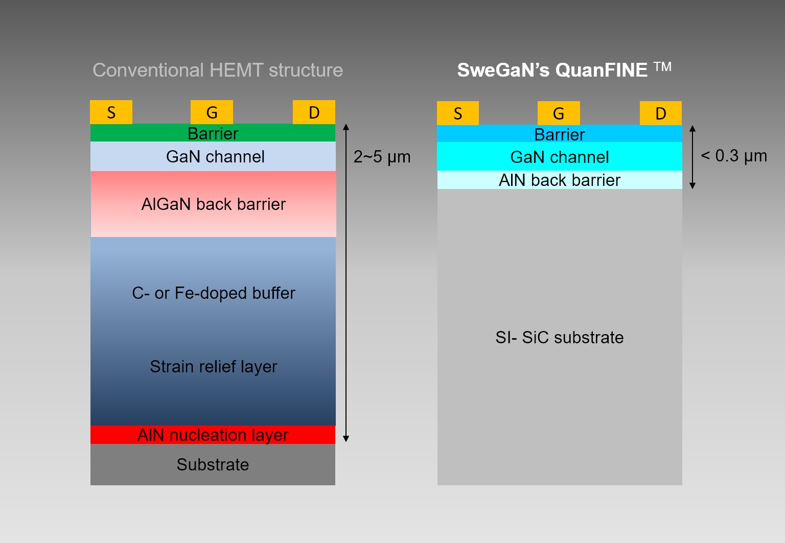
The simplified QuanFINE heterostructure is said to provide superior electrical and thermal properties including low current dispersion, excellent heat dissipation and high breakdown performance, to ensure the best long-term return-on-investment for customer product development for RF and power applications.
”Our new product signals that SweGaN is aligning its production capacity and capability closely with our customers’ needs for the rapidly expanding 5G networks, defence radars and satellite communication, said Jr-Tai Chen, CTO at SweGaN AB. The 150mm QuanFINE product will also facilitate the development of high-end GaN power devices, where price–performance ratio and reliability are critical elements for our customers. ”
Highlighting that device manufacturers typically execute over 100 steps during the fabrication of a device, a larger epiwafer - in simple terms - means manufacturers can produce more devices in the same cycle time, creating clear benefits for return-on-investment.


