
Instrument Systems announces testing station for μLEDs
Efficient, simultaneous testing of thousands of μLEDs on a wafer with a 2D camera system from the LumiTop series
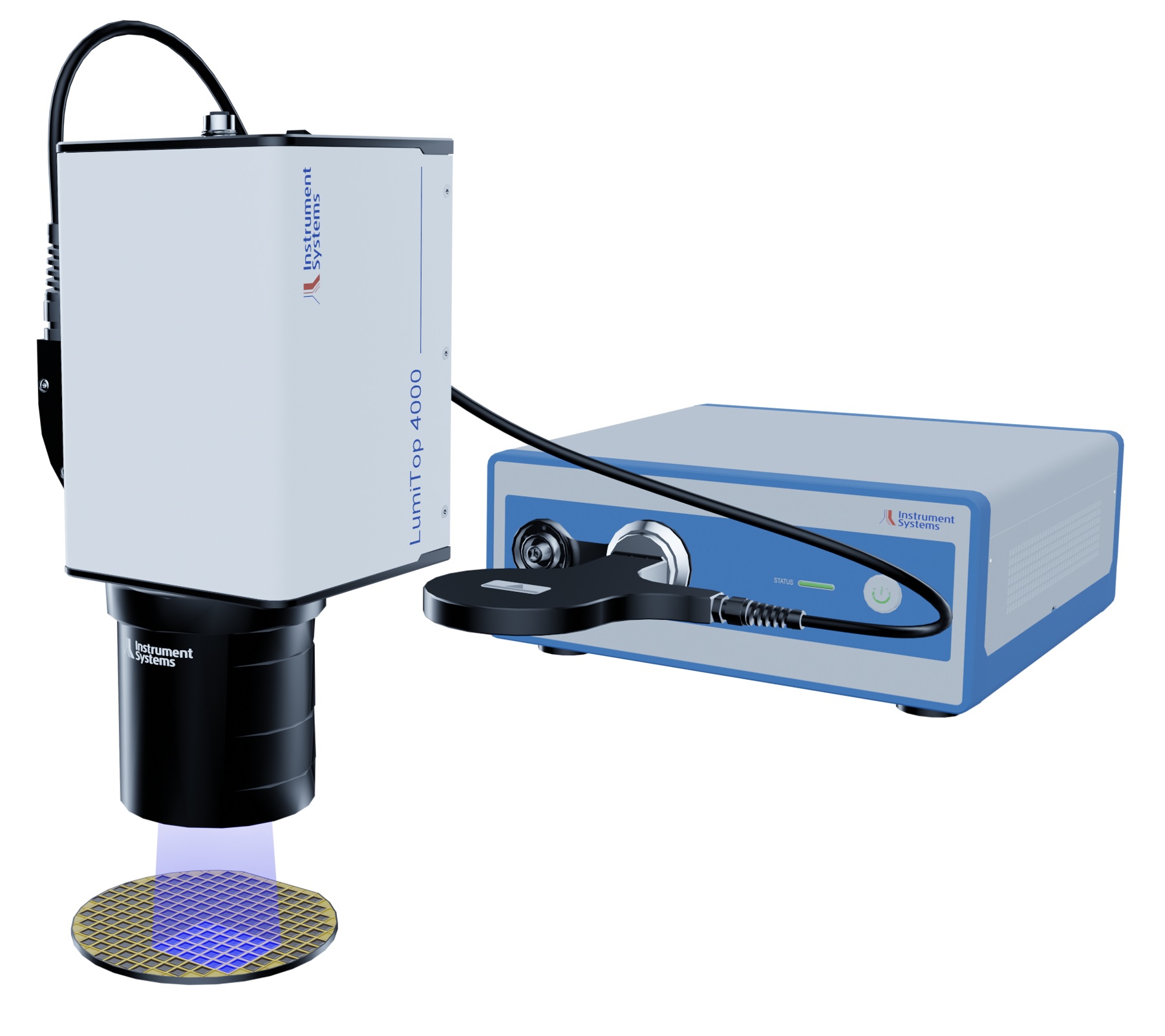
Instrument Systems has announced a camera-based measurement solution for μLED wafer testing that generates 2D, pixel-resolved optical analyses within given cycle times. The LumiTop 4000 has a resolution of 12 MP and can detect the smallest of defects and inhomogeneities on the wafer. Thanks to a 100 mm macro lens, the camera enables fast parallel inline analysis of all μLEDs on a wafer at a single test station.
μLEDs are an exacting new display technology. They are smaller than 100 micrometers and have exceptional optical properties that enable the manufacture of displays with a broad color gamut, high contrast and extremely high resolution. Particularly in mass production, they present new challenges for the optical quality tests required at every stage of production, i.e. including wafer level. This cannot be achieved with standard tests, i.e. sequential testing.
For efficient testing of thousands of μLEDs on a wafer, the test procedure must be done in parallel. The manufacturer is thus required to simultaneously contact as many μLEDs as possible. In addition, the optical inspection should be fast and accurate, and performed synchronous to the production flow. This functions only with a 2D measurement using specifically calibrated instruments to prevent measurement errors.
The 2D camera systems of the LumiTop family from Instrument Systems offer a fast solution that has become established in production. The 2D camera is combined with a high-end spectroradiometer that serves as a simultaneous reference measuring instrument for highly accurate readings. The LumiTop family includes a special version for test objects of all sizes. The new LumiTop 4000 with a 100 mm lens is particularly well suited to μLED wafer testing. With a field of view (FoV) of approx. 1.0 by 1.4 cm it can measure many thousands of μLEDs in parallel with a minimum pixel size as low as 30 micrometers. A hardware trigger synchronises the camera with the given cycle time. The CMOS sensor offers a broad dynamic range.
The accompanying comprehensive LumiSuite software enables wide-ranging analyses of the readings, including the preparation of a pixel intensity map or color map. Algorithms can search for and mark pixel defects according to selectable criteria.


