Scientists build Vertical LED on CMOS-compatible Substrate

Research could contribute to building highly integrated optoelectronics on silicon substrates
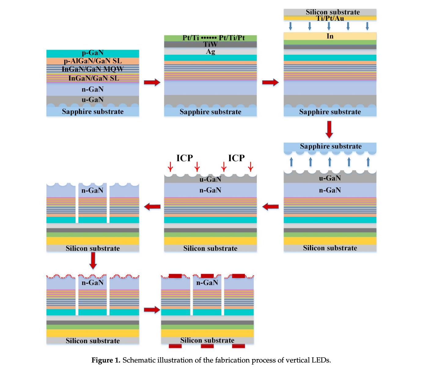
Researchers from Wuhan University in China, in collaboration with the LED company Changelight, have reported developing high optical performance vertical LEDs on CMOS-compatible 4-inch p-type silicon substrate. They achieved this by using highly reflective Ag/TiW metallisation scheme, Au-In eutectic bonding, laser lift-off, and KOH wet etching.
The silicon substrate is compatible with the widely used CMOS circuits. The combination of GaN-based LEDs with silicon based integrated circuits would facilitate the wide application of GaN-based LEDs. “Our finding will contribute to the pursuing of highly integrated optoelectronics on silicon substrates," said Shengjun Zhou who led the WHU team.
Due to lattice and thermal mismatch, the LED structures on sapphire substrate suffer from compressive strain, thus resulting in serious quantum-confined Stark effect (QCSE). In the study, published in crystals, the researchers demonstrated the influence of transferring LED epilayers from a sapphire substrate onto the silicon substrate on the emission characteristics of the vertical LEDs.
The LED epilayers were transferred from a sapphire substrate onto the silicon substrate by Au-In eutectic bonding and laser lift-off. Removing the sapphire substrate can relax the compressive stress in the InGaN quantum well. Furthermore, the relaxation of compressive stress weakens the piezoelectric field. Thus, the band restores towards flat conditions and the overlap area of the electron and hole wave functions increases, alleviating the adverse impacts of QCSE. Hence, the peak emission wavelength blue-shifts and the localised carrier recombination efficiency increases.
The researchers also employed integrated surface textures to improve light extraction efficiency of the vertical LEDs. The integrated surface textures including micro-scale periodic hemispherical dimples and nano-scale random hexagonal pyramids were formed on the surface of the n-GaN after removing patterned sapphire substrate and KOH wet etching. With integrated surface textures, the vertical LEDs also exhibited a more convergent emission pattern.
‘Optical Characterisation of GaN-Based Vertical Blue Light-Emitting Diodes on P-Type Silicon Substrate’ by Yu Lei et al; crystals, Vol. 10, Issue 7, 621(2020).


