
Tyndall Scientists print tiny GaAs PV cells on silicon
Micro transfer-printing technique shows promise for laser power beaming as a way of transferring energy over fibre or free space
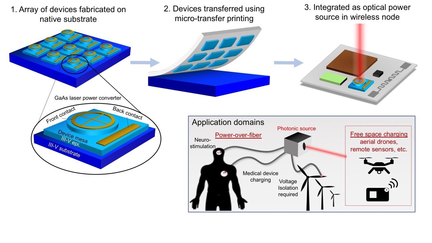
Researchers at the Tyndall National Institute in Cork have demonstrated highly efficient power conversion on silicon substrates under laser light at 808-nm using GaAs based photovoltaic (PV) power convertersAn open circuit voltage of 1.235 V and conversion efficiency of 49 percent was obtained under an equivalent power density of 700 suns. To accomplish this, the cells fabricated on GaAs were removed from their native substrate and transfer-printed to silicon substrates metallised with reflective gold.
Laser power beaming provides a means of transferring energy over fibre or free space to a photovoltaic device in order to power circuitry that must be hermetically sealed or that proves otherwise difficult to connect with traditional electrical power. One example is with implantable biomedical sensors & stimulators where, in order to make them compatible with Magnetic Resonance Imaging, the electric wires need to be eliminated.
In other situations, optical power transmission can ensure voltage isolation can be maintained or lightning safety for wind turbine blade monitoring and underwater robotics. There are also a wide range of embedded systems that operate in harsh industrial environments that would benefit from minimised electromagnetic interference.
The most efficient PV devices are based on III-V materials while electronics components are based on silicon and thus dissimilar materials and devices need to be integrated to benefit from the properties of each. Micro-transfer-printing (μTP) provides a means to intimately integrate the micron-thick essential layers of GaAs photovoltaic power converters with Si circuits.
The μTP approach allows the re-use of the growth substrate providing a financial and environmental incentive. In addition, the power supplied by environmental energy harvesters is typically restricted to the micro-watt range, limiting the functionality of connected systems whereas sub mm-scale laser power converters are capable of supplying 10s of mW to potentially watts of power. Here, the team applied the μTP technique to produce laser power converters that deliver 44 mW with a 300-μm diameter cell. This high-power delivery opens up the possibility of powering complex sensors and computational systems at the edge, enabling edge AI applications in power-over-fibre systems.
The PV converter was grown on a GaAs wafer by MOVPE with a p-on-n epitaxial structure consisting of a thin GaAs emitter and thick GaAs base with AlGaAs current spreading layers on both sides. An Indium Tin Oxide (ITO) layer was deposited to reduce the resistance caused by limited lateral current spreading at high currents. The first layer in the epi-structure is a 500-nm thick lattice matched AlInP etch release layer which allows the undercut of the fabricated devices in dilute hydrochloric acid.
To enable the systematic release and transfer of the devices, a compatible photoresist tethering system was used that allowed the release of devices that are then suspended and held in place once undercut. This allows registered pick and print of the devices onto the target silicon substrate with a PDMS elastomer stamp. The gold coated silicon acted as a mirror reflecting unabsorbed photons back towards the junction. The thin active layer results in photon recycling which increases the carrier density, thus increasing the open circuit voltage of the device.
The device efficiency can be improved further by optimising the epitaxial design, light management and current collection under high bias. Particularly, the grid pattern on the device in conjunction with transparent current spreading layers could be optimised to reduce the shadowing effect of the grid while reducing the resistance caused by the lateral currents.

(The picture above is an optical microscope image of a 300 μm diameter device during EL measurements. The schematic at the top shows fabrication and micro transfer printing of on-chip III-V optical power sources and the potential applications of the technology including power-over-fibre and free space optical charging.)
'Micro-transfer printing high-efficiency GaAs photovoltaic cells onto silicon for wireless power applications' by Ian Mathews et al; Advanced Materials Technologies, 6th July 2020


