
Flexible micro LEDs can be folded, cut and stuck to surfaces
University of Texas at Dallas researchers make novel LED using remote epitaxy
University of Texas at Dallas researchers and their international colleagues have developed a method to create micro LEDs that can be folded, twisted, cut and stuck to different surfaces. The research, published online in June in the journal Science Advances, helps pave the way for the next generation of flexible, wearable technology.
Micro LEDs, which can be as small as 2 micrometers and bundled to be any size, provide higher resolution than other LEDs. Their size makes them a good fit for small devices such as smart watches, but they can be bundled to work in flat-screen TVs and other larger displays. LEDs of all sizes, however, are brittle and typically can only be used on flat surfaces.
The researchers' new micro LEDs aim to fill a demand for bendable, wearable electronics.
"The biggest benefit of this research is that we have created a detachable LED that can be attached to almost anything," said Moon Kim, Louis Beecherl Jr. distinguished professor of materials science and engineering at UT Dallas and a corresponding author of the study. "You can transfer it onto your clothing or even rubber -- that was the main idea. It can survive even if you wrinkle it. If you cut it, you can use half of the LED."
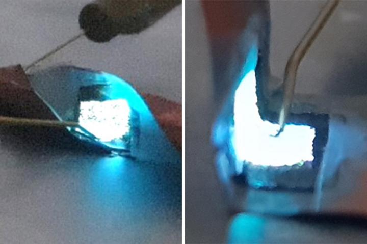
Researchers in the Erik Jonsson School of Engineering and Computer Science and the School of Natural Sciences and Mathematics helped develop the flexible LED through remote epitaxy by growing a thin layer of LED crystals on the surface of a sapphire crystal wafer.
Typically, the LED would remain on the wafer. To make it detachable, researchers added a nonstick layer of graphene to the substrate.
"The graphene does not form chemical bonds with the LED material, so it adds a layer that allows us to peel the LEDs from the wafer and stick them to any surface," said Kim, who oversaw the physical analysis of the LEDs using an atomic resolution scanning/transmission electron microscope at UT Dallas' Nano Characterisation Facility.
Colleagues in South Korea carried out laboratory tests of LEDs by sticking them to curved surfaces, as well as to materials that were subsequently twisted, bent and crumpled. In another demonstration, they adhered an LED to the legs of a Lego minifigure with different leg positions.
Bending and cutting do not affect the quality or electronic properties of the LED, Kim said.
The bendy LEDs have a variety of possible uses, including flexible lighting, clothing and wearable biomedical devices. From a manufacturing perspective, the fabrication technique offers another advantage: Because the LED can be removed without breaking the underlying wafer substrate, the wafer can be used repeatedly.
"You can use one substrate many times, and it will have the same functionality," Kim said.
In ongoing studies, the researchers also are applying the fabrication technique to other types of materials.
"It's very exciting; this method is not limited to one type of material," Kim said. "It's open to all kinds of materials."
'Remote heteroepitaxy of GaN microrod heterostructures for deformable light-emitting diodes and wafer recycle' by Junseok Jeong et al; Science Advances 03 Jun 2020; Vol. 6, no. 23,


