Loading...
News Article

Hamamatsu Photonics completes new factory

News

New building at Shingai factory site will help streamline opto-semiconductor device production and increase capacity

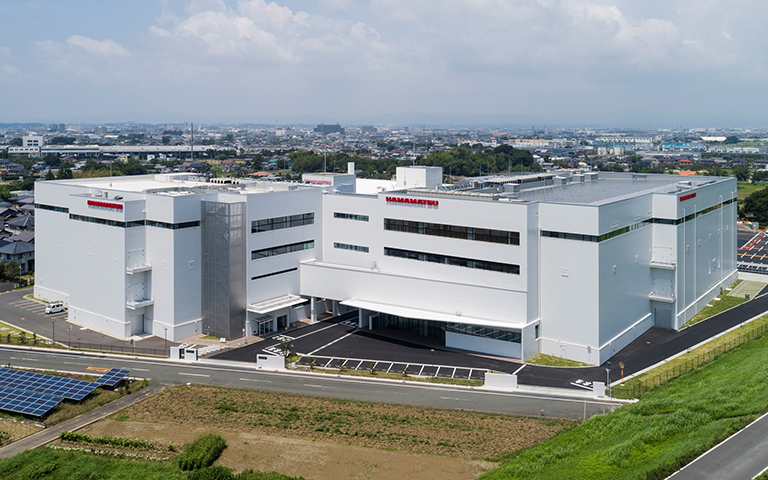
Hamamatsu Photonics has announced the completion of a new building at its Shingai Factory, Japan to cope with increasing sales demand for opto-semiconductors, X-ray image sensors and X-ray flat panel sensors. The new factory building will start operations in October this year.

Hamamatsu Photonics has been supplying opto-semiconductor products for a wide range of applications and fields such as medical diagnosis and treatment, industrial instrumentation, automotive, and scientific measurement.

Recently, there has been an increasing demand for plastic-moulded opto-semiconductors mass-producible in large quantities, as well as for X-ray image sensors and X-ray flat panel sensors used in radiation inspection devices.

Construction of this new factory building will help the company not only increase production but also allow it to consolidate opto-semiconductor production processes that are currently located separately from each other at the Shingai Factory and associated companies.

To boost X-ray image sensor and X-ray flat panel sensor production, Hamamatsu says it will speed up product development by consolidating design, development and evaluation into a single area and will also streamline our supply system by way of production processes located on the same floor to respond to growing demand.

The new building incorporates earthquake and flood control measures as well as eco-friendly measures such as LED lighting, heat-insulated walls, solar power plant, and rainwater reuse systems.

SiC MOSFETs: Understanding the benefits of plasma nitridation
Wolfspeed reports Q2 results
VueReal secures $40.5m to scale MicroSolid printing
Mitsubishi joins Horizon Europe's FLAGCHIP project
Vishay launches new high voltage SiC diodes
UK team leads diamond-FET breakthrough
GaN adoption at tipping point, says Infineon
BluGlass files tuneable GaN laser patents
QD company Quantum Science expands into new facility
Innoscience files lawsuit against Infineon
Riber revenues up 5% to €41.2m
Forvia Hella to use CoolSiC for next generation charging
Photon Design to exhibit QD simulation tool
Ortel transfers CW laser fabrication to Canada
Luminus adds red and blue multi-mode Lasers
PseudolithIC raises $6M for heterogeneous chiplet tech
Mesa sidewall design improves HV DUV LEDs
IQE revenue to exceed expectations
'Game-changing' VCSEL system targets clinical imaging
German start-up secures finance for SiC processing tech
Macom signs preliminaries for CHIPS Act funding
IQE and Quintessent partner on QD lasers for AI
EU funds perovskite tandems for fuel-free space propulsion
EU to invest €3m in GeSi quantum project
Transforming the current density of AlN Schottky barrier diodes
Turbocharging the GaN MOSFET with a HfO₂ gate
Wolfspeed launches Gen 4 SiC MOSFET technology
Report predicts high growth for UK's North East
Element Six unveils Cu-diamond composite
SemiQ launches hi-rel 1700V SiC MOSFETs
Lynred to exhibit Eyesential SWIR sensor for machine vision
Thorlabs buys VCSEL firm Praevium Research
×
Search the news archive

To close this popup you can press escape or click the close icon.
Logo
x
Logo
×
Register - Step 1

You may choose to subscribe to the Compound Semiconductor Magazine, the Compound Semiconductor Newsletter, or both. You may also request additional information if required, before submitting your application.


Please subscribe me to:


You chose the industry type of "Other"

Please enter the industry that you work in: