Loading...
News Article

Samco launches PECVD and ALD demo facility

News

Kyoto-based facility will include ten PECVD and ALD systems to support growth of deposition and coating business

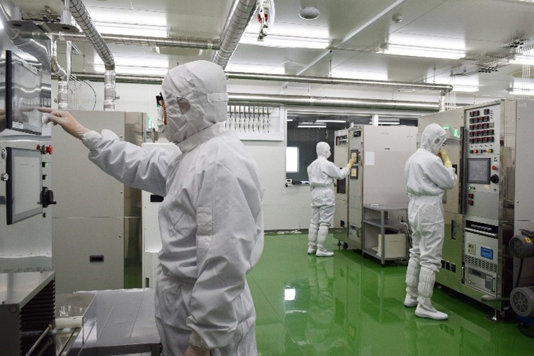
Samco, a manufacturer of plasma processing equipment for the compound semiconductor industry, has announced the opening of its new PECVD and Atomic Layer Deposition (ALD) demonstration facility at Samco’s headquarters, Kyoto, Japan.

Samco’s PECVD and ALD systems are used for manufacturing optoelectronic and electronic devices. The rapid growth of the 5G and IoT markets has fuelled demand for PECVD and ALD process equipment.

“This new facility is of strategic importance to Samco as it will enable further revenue growth in the compound semiconductor market. There will be ten PECVD and ALD systems for demonstration in the class 1000 cleanroom space of 217.61 m2,” says Tsukasa Kawabe, Samco’s president and COO.

“The facility will greatly strengthen our ability to develop future process applications and technologies with our customers across the globe. The volume of demonstration tests requested by customers that can be handled is expected to be more than double the current level. Moreover, our customers and partners could collaborate with us in prototyping and pilot-line production utilising the new facility,” he adds. “In particular, we are planning on conducting joint research and development projects with universities, research institutes, companies, and other external parties more aggressively than ever.”

“Samco’s three pillars of core technology are deposition, etching, and surface cleaning. We will leverage this new facility to further expand sales of the PECVD and ALD systems,” says Kawabe.

SiC MOSFETs: Understanding the benefits of plasma nitridation
Wolfspeed reports Q2 results
VueReal secures $40.5m to scale MicroSolid printing
Mitsubishi joins Horizon Europe's FLAGCHIP project
Vishay launches new high voltage SiC diodes
UK team leads diamond-FET breakthrough
GaN adoption at tipping point, says Infineon
BluGlass files tuneable GaN laser patents
QD company Quantum Science expands into new facility
Innoscience files lawsuit against Infineon
Riber revenues up 5% to €41.2m
Forvia Hella to use CoolSiC for next generation charging
Photon Design to exhibit QD simulation tool
Ortel transfers CW laser fabrication to Canada
Luminus adds red and blue multi-mode Lasers
PseudolithIC raises $6M for heterogeneous chiplet tech
Mesa sidewall design improves HV DUV LEDs
IQE revenue to exceed expectations
'Game-changing' VCSEL system targets clinical imaging
German start-up secures finance for SiC processing tech
Macom signs preliminaries for CHIPS Act funding
IQE and Quintessent partner on QD lasers for AI
EU funds perovskite tandems for fuel-free space propulsion
EU to invest €3m in GeSi quantum project
Transforming the current density of AlN Schottky barrier diodes
Turbocharging the GaN MOSFET with a HfO₂ gate
Wolfspeed launches Gen 4 SiC MOSFET technology
Report predicts high growth for UK's North East
Element Six unveils Cu-diamond composite
SemiQ launches hi-rel 1700V SiC MOSFETs
Lynred to exhibit Eyesential SWIR sensor for machine vision
Thorlabs buys VCSEL firm Praevium Research
×
Search the news archive

To close this popup you can press escape or click the close icon.
Logo
x
Logo
×
Register - Step 1

You may choose to subscribe to the Compound Semiconductor Magazine, the Compound Semiconductor Newsletter, or both. You may also request additional information if required, before submitting your application.


Please subscribe me to:


You chose the industry type of "Other"

Please enter the industry that you work in: