
Trilayer of GaAs enhances terahertz performance
A trilayer structure incorporating a thin n-doped buffer yields a promising performance as both a detector and emitter
A collaboration between researchers at the University of the Philippines and the University of Fukui has developed a trilayer GaAs structure that enhances terahertz emission and detection.
The team’s device, featuring a layer grown at low-temperature and a thin n-doped buffer, delivers a superior emitter and detector performance to a variant with an undoped buffer.
This effort supports the development of semiconducting materials that are already used to generate and detect terahertz emission in commercial systems. Semiconductors provide ultrafast switching in photoconductive antenna deployed in terahertz imaging and spectroscopy systems.
When GaAs is used in terahertz systems, it is grown at lower temperatures. “[GaAs’] short carrier lifetime makes it more relevant as a terahertz detector,” says researcher Elizabeth Ann Prieto. “GaAs grown at a high or conventional temperature is effective as terahertz emitter but is not suitable as a terahertz detector.”
The effectiveness of low-temperature-grown GaAs as terahertz emitter depends on its level of crystallinity, while the capability of the detector is governed by the shortness of its carrier lifetime. Unfortunately, it’s not possible to excel on both fronts with a single layer of GaAs grown at a low temperature.
“As the growth temperature of GaAs is lowered, its crystallinity deteriorates while its carrier lifetime shortens”, says Prieto. This makes conventional, low-temperature-grown GaAs inferior as a terahertz emitter but effective as a terahertz detector.
By turning to a doped buffer, the team is able to make low-temperature-grown GaAs effective as terahertz emitter. “The cons have been eliminated by making the low-temperature-grown GaAs layer thick while making the doped buffer layer thin,” explains Prieto.
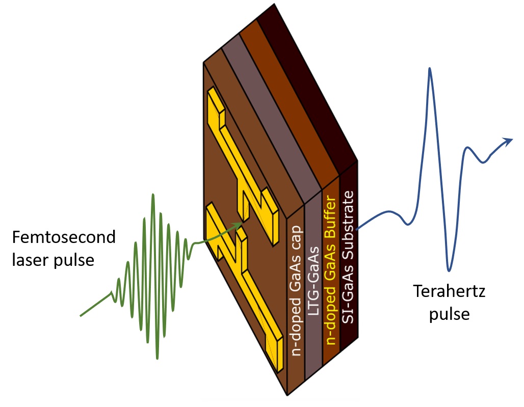
The team produces its devices by taking a 600 µm-thick semi-insulating GaAs substrate, loading it into the growth chamber of a solid-source Riber 32P MBE reactor, and depositing three layers of GaAs.
Growth begins with a 0.2 µm-thick, n-doped GaAs buffer, grown at 630degC. After this, Prieto and co-workers add a 2 µm-thick active layer grown at just 270degC, prior to annealing at 600degC; followed by a 20 nm-thick n-type GaAs cap, grown at 600degC.
To assess this structure, the researchers also produced a structure with an undoped GaAs buffer.
Metal contacts were added using standard photolithography processes, sequentially involving wafer cleaning, photoresist application, soft baking, mask alignment, UV exposure and development.
For contact lithography of the photoconductive antenna, the team used a positive photoresist and a mask aligner.
Using these processes, the researchers created a Hertzian dipole antenna consisting of two metal electrodes, separated by a 5 µm gap.
The team turned to a standard terahertz time-domain spectroscopy system to form the terahertz emitter and detector. A fibre laser operating at 780 nm and delivering 100 fs pulses with a 100 MHz repetition rate provided the optical excitation source.
Both types of device produced emission extending up to around 3 THz, as is to be expected with a structure formed from low-temperature GaAs featuring a Hertzian dipole antenna. For frequencies of around 1 THz and above, there is a drop in output power of an order of magnitude between the doped and undoped structures when excited with a pump power of 0.8 mW. Comparing peak-to-peak terahertz emission intensity, the doped sample provided an increase of 116 percent.
As a detector, the doped sample provided a dynamic range of 55 dB at 0.5 THz, a figure 5 dB higher than the undoped control.
(The figure above shows the trilayer GaAs structure incorporating a doped buffer).
Prieto and co-workers are planning to fabricate more prototypes to bring the technology closer to deployment.
More details on this work are described in the paper 'Trilayer low-temperature-grown GaAs terahertz emitter and detector device with doped buffer' by E. A. Prieto et al; Appl. Phys. Express 13 082102 (2020).


