
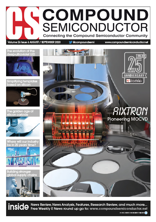
Masterful MOCVD manufacture
With a pedigree dating back to the early 1980s, Aixtron has spent several decades at the forefront of MOCVD equipment manufacturing
BY MICHAEL HEUKEN FROM AIXTRON
BACK IN 1995, when Compound Semiconductor magazine made its debut, Bill Clinton presided over the United States, owners of PCs could start getting their hands on Windows 95, and our industry was far, far smaller than it is today.
Reflecting its diminutive size was its lack of diversity. This is illustrated by the narrowness of the discussion that took place at the 8th ICMOVPE, held in Cardiff in 1996, where delegates pondered the question “MOVPE – Is there any other technology for optoelectronics?”. Back then the manufacture of red and infrared LEDs was well established, but the blue cousin had only just been invented; volumes of GaAs HBT production were tiny, due to very few owners of mobile phones; III-V solar cells were yet to establish themselves as the dominant technology for powering satellites; and the manufacturer of InP lasers and photodetectors to build the information superhighway provided a substantial proportion of total industry revenue.
Although the compound semiconductor industry was in its infancy back then, manufacturers of optoelectronic devices did not have to rely on home-built systems for MOCVD growth. They also had the option of purchasing commercial reactors.
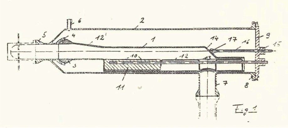
Figure 1. On the 30 June 1987 Aixtron co-founder Holger Jürgensen and his colleague Meino Heyen filed a German patent for the invention of a horizontal tube reactor, later marketed as Aixtron 200. This patent, published on 12 January 1989, details a round outer tube and an inner rectangular liner tube. The design allows an easy exchange of the liner, aiding cleaning. The susceptor is positioned parallel to the gas flow. In the patent there is a diagram of the reactor, shown above, and labelled: (1) inner rectangular quartz reactor, (2) round outer quartz tube for protection, (3) flange with spherical connector, (4) flange to pick up the connector of the rectangular quartz reactor, (5) gas inlet for process gases, (6) purge gas inlet, (7) exhaust, (8) reactor port seal, (9) reactor port for loading and liner tube exchange, (10) wafer, (11) susceptor as wafer carrier, (12) quartz plate to maintain laminar flow, (13) exhaust opening, (14) reactor end to optimise flow, (15) screw joint to adjust the liner tube with the push rod, (16) push rod, and (17) fixing for the push rod.
Leading the supply of such tools is our company, Aixtron of Aachen, Germany. Founded in 1983 as a spin-off of RWTH Aachen University, by 1995 we were a well-established business, offering refined products. A foundation for this success is a key patent, issued in 1989, that details a horizontal tube quartz reactor (see Figure 1).As far back as the 1980s, we had started to consider the limitations of our first commercial reactors, the Aixtron 200 series (see Figure 2, 3 and 4. The latter shows a typical reactor from the Aixtron 200 series, the Aixtron 200/4 system, which features heating with a standard lamp or an RF heating system, a glove box and computer control.). Reactors in the Aixtron 200 series had been prototyped at RWTH, prior to further development and commercialisation by our team. This MOCVD system had a great reputation within the research community, thanks to its combination of simplicity, reliability, versatility and ease of use.
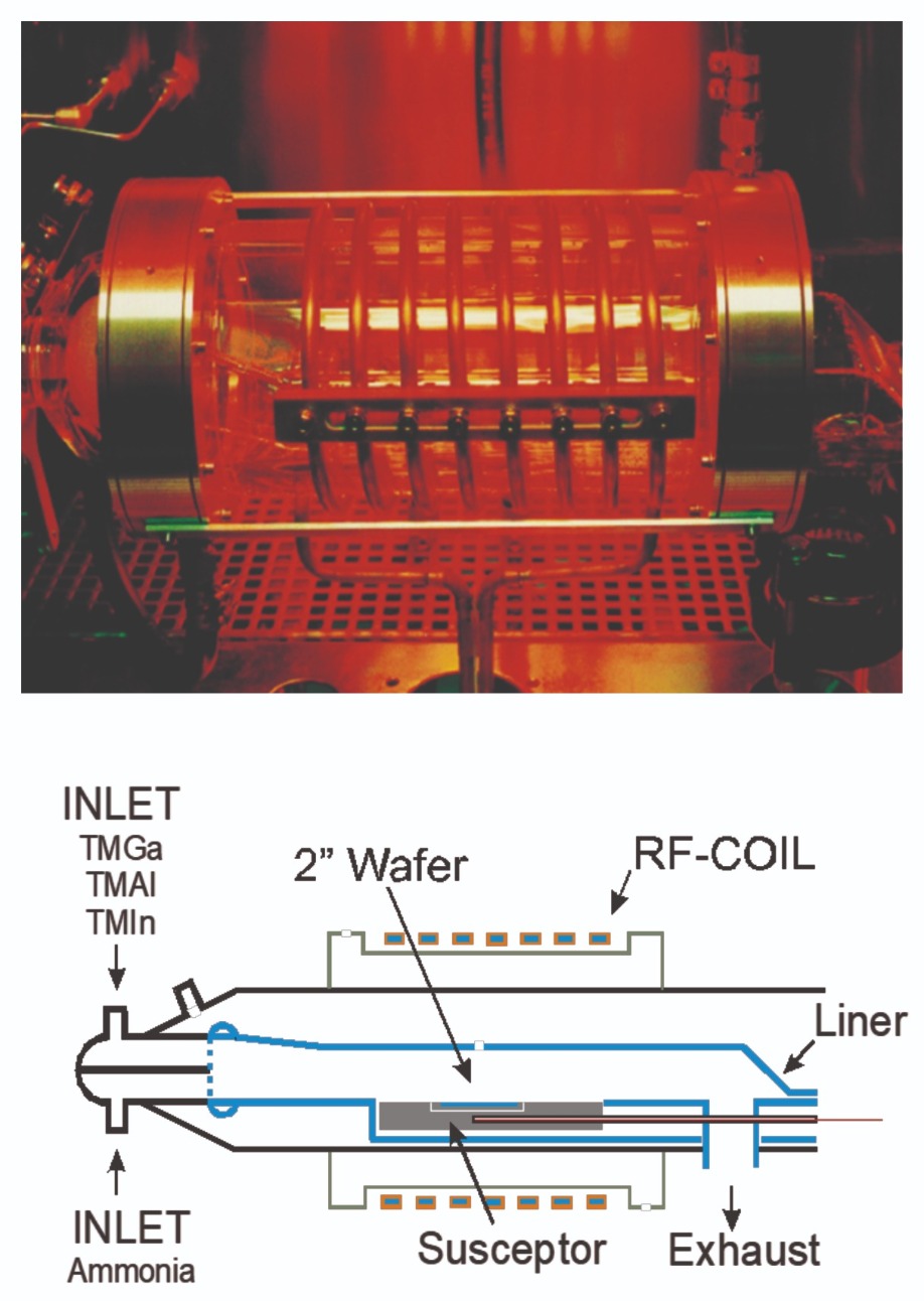
Figure 2. (a) A horizontal tube 200 reactor with water cooling, suitable for high-temperature growth. The RF coil allows heating well above 1000 °C, enabling the growth of III-N based materials. (b) A diagram of the 200 reactor, showing the holes in the liner tube. The transparency of these quartz reactors provided some of the first in-situ monitoring during growth.
Scientists and engineers employed this reactor for the growth of a wide variety of epitaxial layers, from III-V compounds, such as As/P/Sb based material systems, to wide bandgap II-VI compounds, which included ZnSe and ZnMgSe. The latter pair held much promise for commercial blue LEDs and lasers. But the Aixtron 200 did not address the needs of engineers in industry, who were working hard to develop processes for high-volume production of epiwafers.A severe limitation of the horizontal tube reactor is its side walls. When they are hot heterogeneous reactions take place; and when they are cold condensation forms. Another impediment is that the side walls consume source material, impairing the efficiency and the uniformity of the reactor. The side walls also alter the flow pattern perpendicular to the gas flow direction, making the growth of high-quality epilayers more difficult.
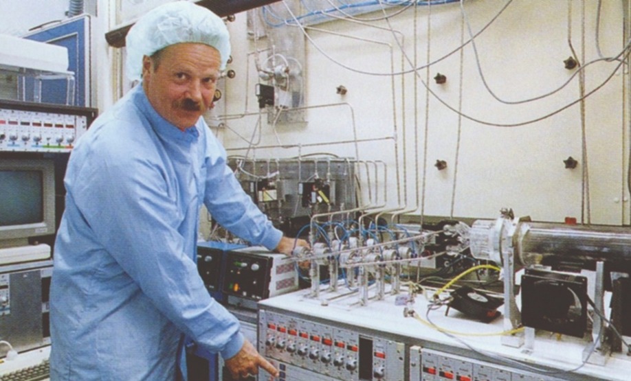
Figure 3. Holger Jürgensen, co-founder of Aixtron, operating one of the company’s first prototype reactors, used at that time for the growth of InP materials at RWTH Aachen University. The early work was undertaken in co-operation with D. Grützmacher, today professor at FZ Jülich. The image shows the quartz reactor, early versions of the vent run system and so-called read out boxes to set the mass-flow control (MFC) readings. Fans under the reactor were switched on in the cool down phase to decrease cool down time and increase productivity. Picture from late 1980s.
Horizontal tube reactors are also unsuitable for high throughput, because this architecture is hard to scale to multiple, large-diameter wafers. In practice, the highest production volumes are limited to a single 4-inch wafer, using growth rates no more than 1 μm/hr.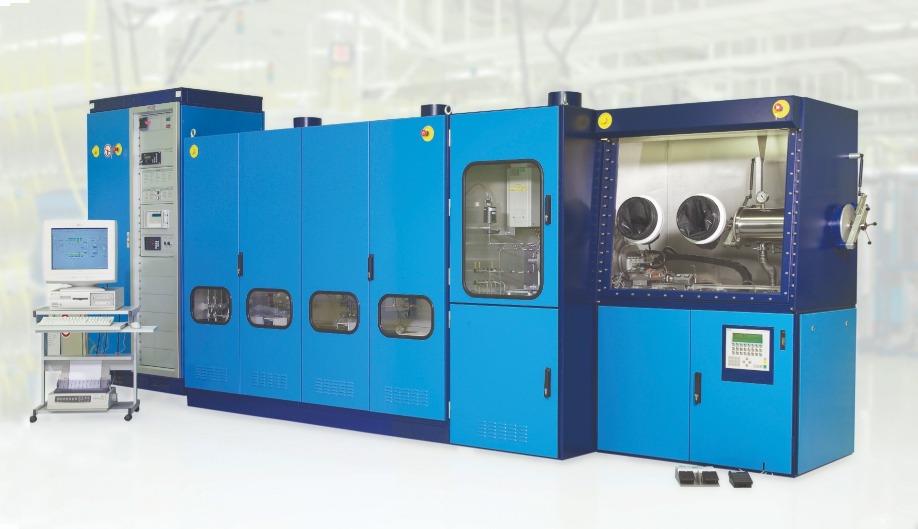
Figure 4. Standard lamp-heated Aixtron 200/4 system with the typical blue colour, glove box and computer control. This reactor was used primary for growing GaAs- and InP-based material systems. One wafer up to 4 inch fits into the reactor.
To address the increasing demands of high-volume chipmakers needing to fulfil ever-tighter specifications in a broadening range of applications, we launched a range of multi-wafer reactors. The first of this new breed of reactor, the AIX 2000 Planetary Reactor series, debuted in the late 1980s/early 1990s. Sales took off, with engineers using it to make many different devices, including InP lasers, red LEDs, space solar cells and the first commercially available HBT to be grown by MOCVD.Planetary Reactor
Demand for compound semiconductor devices continued to rise throughout the 1990s and beyond. We responded with the introduction of our Planetary Reactor series, which uses two forms of circular motion to ensure the uniformity of many wafers in a reactor. Every wafer rotates around the centre of the reactor, and clusters of them also circulate around their own local centre (see Figure 5).
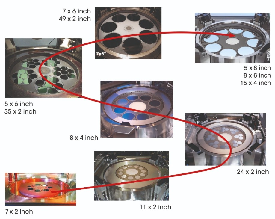
Figure 5. The evolution of the Planetary Reactor family for the growth of III-N material. Based on simulation results, reactor chambers became larger, accepting more and larger wafers, while simultaneously improving uniformity and reducing material consumption per wafer area.
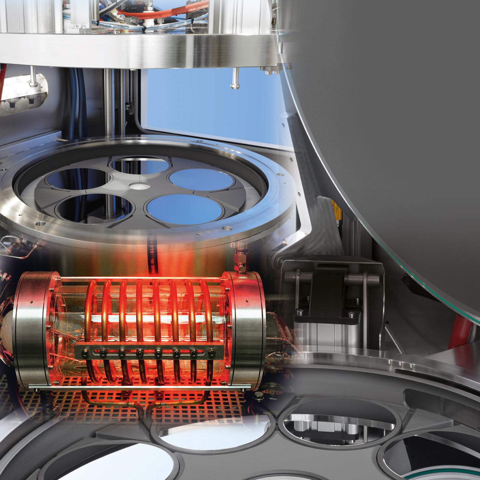
The inventor of the Planetary Reactor, Peter Frijlink, came up with the idea while working at Philips Research Sureness, France. His design targeted the growth of GaAs/AlGaAs heterostructures and he filed a patent entitled Planetary reactor for epitaxy in late 1980s (details of his design are given in his paper A new versatile large size MOVPE reactor, published in Journal of Crystal Growth 93 207 (1988)). A grant for the patent came through in the early 1990s. We acquired a license to use this unique idea of the planetary motion of substrates, and then went on to further develop the technology. Our first Planetary Reactor used lamp heating, but we switched to RF heating systems to realise higher growth temperatures and ensure faster heating cycles, which increase production (some of early reactors are shown in Figures 5-9).The Planetary Reactor has many merits. It is a horizontal reactor which is free from side walls, and the temperature of its top wall, also known as the ceiling, can be controlled to make it passive. This type of reactor can ensure excellent, controllable uniformity, making it ideal for large scale production. It is also renowned for its: high precursor utilisation efficiency; its low maintenance requirements; its accommodation of large wafer areas; the opportunity it provides to use automated cassette-to-cassette loading systems; and its high growth rates – values of more than 30 μm/hr. Thanks to this great set of attributes, our Planetary Reactors provide low-cost, high-volume, multi-wafer production using multiple wafers up to 200 mm.
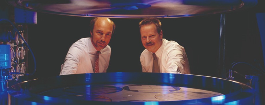
Figure 6. The 1995 Aixtron top management team: Dr. Holger Jürgensen and Kim Schindelhauer. They are looking into the Planetary Reactor of the 3000 series developed for large-area, GaAs-based solar cells.
By comparing the early 200 reactor series with today’s Planetary Reactors, we can see the tremendous strides that we have made over the last 25 years in yield, productivity and cost. One way to evaluate this is to consider LED production, plotting the fall in the cost-per-kilolumen and the increase in the total daily epiwafer area. We have done just this, considering our leading reactors between 2000 and 2016 (see Figure 10). Increases in performance have been driven by improvements in reactor technology. That has led to a higher yield from each process run. Improvements in MOCVD technology are also behind the cutting of the cost-per-kilolumen, which has also fallen in with more efficient LED designs.In the 2000s, the increases in yield that drove the cost reductions that are shown in Figure 10 came through accommodating a larger wafer area in the reactor, while keeping uniformity as high as possible. Launched in 2001, our third-generation Planetary Reactor for GaN, the AIX 2400 G3, had a capacity of 11 2-inch wafers. Upgrading this the following year led to the introduction of the AIX 2600 G3, which could accommodate 24 2-inch wafers. By 2006, we could house 42 2-inch wafers, thanks to the launch of the AIX 2800 G4 HT, a fourth-generation GaN Planetary Reactor. The first fifth-generation GaN Planetary Reactor followed in 2009, enabling growth of 8 6-inch epiwafers in a single run. During the last decade increases in productivity have not come from increases in wafer capacity, but from other strategies that trim cycle times, such as the introduction of automated wafer-loading systems.
We have been working on wafer loading for many years. Back in 1996 we developed the first automated MOCVD reactor, featuring a spider-like robot for loading wafers into a cassette. By avoiding the need to cool wafers to room temperature, this handler cut cycle times by up to 30 percent, increasing throughput.
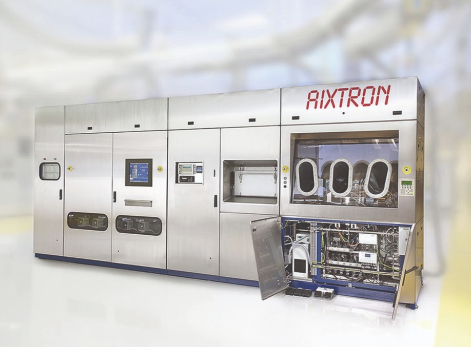
Figure 7. The Planetary Reactor in the integrated concept design. Beside productivity improvements, the stainless steel outlook approaches silicon fab style.
Even shorter cycle times resulted from the introduction of cassette-to-cassette loading of hot wafers (Figure 11 shows our latest G5+ C dual Planetary Reactor module cluster, equipped with cassette-to-cassette wafer handling). By turning to hot wafer loading we slashed the process cycle time by up to 50 percent for specific applications. To increase uniformity and yield further we use a gas-driven wafer carrier (satellite) rotation to track and tune the surface temperature of every wafer individually. Control of the temperature is realised by adjusting the ratio of nitrogen-to-hydrogen rotation gas, a technique that also offers temperature uniformity control for each wafer individually. By applying a software-based automatic correction of the gas flow to individual satellites, we allow engineers to minimise the mean surface temperature deviation for each wafer, for each process step. This technique provides single-wafer reactor uniformity at low multi-wafer reactor cost.A significant refinement to our reactors came in 2012 when we replaced our conventional, triple injectors with variants featuring five injectors. These ‘penta’ injectors brought knew tuning potential to widen the process window for best uniformities up to 200 mm wafer size.
Another aid to the process engineer has been the introduction of optical in-situ monitoring tools. This form of instrumentation opens the door to advanced process control. It enabled logging and control of far more data, including values for wafer bow, growth rate and local on-wafer temperature. By designing reactors that accommodate an optical path to the growth surface, we established emissivity-corrected pyrometry that provides measurements of on-wafer temperature. Armed with this insight, process engineers can now realise wafer level control and optimise their epitaxial yield.
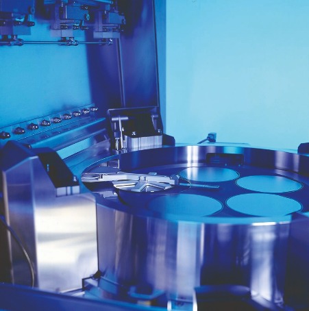
Figure 8. View in an AIX 2600 G3 Planetary Reactor equipped with a wafer loader as delivered in 1996.
It is inevitable for all kinds of reactor designs that the running of an MOCVD process leads to a build-up of III-Vs on the surfaces of the reactor. Eventually they have to be cleaned off, to prevent imperfections on the wafers. Ideally this is automated and well-controlled, as that saves time and enhances reproducibility. As early as 2005, we had technologies in place for a complete, automatic reactor clean after each process run. Initially, our processes were for cleaning InP reactors used for the growth of epiwafers for advanced lasers. About ten years on, we had successfully transferred this concept to III-nitrides.In addition to our portfolio of Planetary Reactors, we offer those that are based on a Closed Coupled Showerhead design. This alternative reactor architecture, developed in parallel, also offers proven production capability. We offer this design to cater to those customers that are more familiar with the Closed Coupled Showerhead reactor and want to continue to produce epiwafers with this technology.
The Closed Coupled Showerhead
Like our Planetary Reactors, within the suite of Closed Coupled Showerhead designs, throughout the first decade of this century increases in wafer capacity led to breakthroughs in productivity. In 2001 and 2002 we launched reactors for nitride growth that accommodated 6 and then 19 2-inch wafers, and we followed this up with the introduction of the Crius, Crius II and Crius II XL in 2006, 2011 and 2012 – they housed 31 2-inch wafers, 55 2-inch wafers, and 19 4-inch wafers, respectively. In 2015, we introduced a semi-automated reactor with an even larger chamber, capable of producing 31 4-inch epiwafers in a single run. With this class of reactor, growth rates of even up to 280 μm/hr were demonstrated.
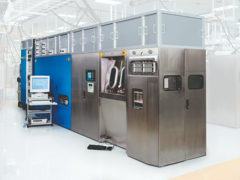
Figure 9. An early Planetary Reactor.
During our time in the compound semiconductor industry, we have witnessed a change in the priorities of our customers. Initially technology drove the market, but this changed around 2011, when cost reigned supreme. For ‘simple’ devices, such as LEDs offering acceptable brightness, many chipmakers wanted low-performance, low-cost equipment offering limited, specialised performance. By 2016 this had created a solid-state lighting market that operated at very thin margins and had little interest in high-end technology.We decided to focus on our strength, which is providing the growth technology for producing high-tech devices that demand advanced MOCVD capability. For engineers that are producing lasers, III-V solar cells, advanced transistors, microLEDs for displays, and high-speed InP-based lasers for telecom and datacom networks, our Planetary Reactors are a great choice, combining a high level of performance with excellent yield and productivity. The Close Coupled Showerhead remains the solution of choice for R&D systems or for single systems that then require superior performance once again – which a vertical batch reactor can inherently not deliver well.
For the last quarter of a century, we have focused on ways to enhance productivity. This has been accomplished through the likes of increased reproducibility, superior layer uniformity, wafer level automation, and the introduction of in-situ metrology that enables the acquisition of process data, key to smart system control and predictive maintenance.
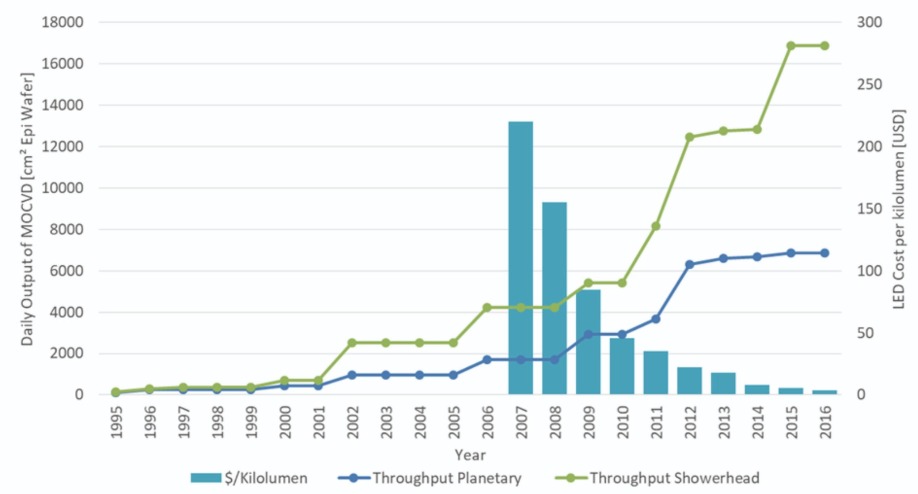
Fig. 10: Progress of MOCVD productivity and cost/kilolumen, based on United States dollars. Calculations used Aixtron estimates and data from https://archive.thinkprogress.org/5-charts-that-illustrate-the-remarkable-led-lighting-revolution-83ecb6c1f472/ The leaps in performance of the Planetary Reactor are due to: the introduction of the 3rd Generation GaN Planetary Reactor AIX 2400 G3 (11 x 2-inch) in 2001; an upgrade to the GaN Planetary Reactor AIX 2600 G3 (24 x 2-inch) in 2002; the launch of the 4th Generation GaN Planetary Reactor AIX 2800 G4 HT (42x2 inch) in 2006; the introduction of 5th Generation GaN Planetary Reactor AIX 2800 G5 HT (8 x 6-inch) in 2009; the implementation of semi-automated wafer loading in 2011; and the switch to a penta injector, for the 5 x 8-inch configuration in 2012. Between 2010 and 2015, additional improvements came from CIP continuous improvement programmes, and the development of chamber in-situ clean. For the closed-coupled-showerhead, productivity gains came from: the introduction of the 6 x 2-inch nitride reactor in 2001; an increase in capacity to 19 x 2-inch in 2002; launches of the Crius, Crius II and Crius II XL in 2006, 2011 and 2012, that had chambers accommodating 31 x 2-inch, 55 x 2-inch and 19 x 4-inch wafers, respectively; and the introduction of the AIX R6, 31 x 4-inch reactor in 2015.
We will continue to innovate our MOCVD process technologies, drawing on learnings from other industry sectors, such as artificial intelligence, and apply this to the analysis of collected data. Another breakthrough could be the introduction of MOCVD 4.0 concepts, a step that could further minimise energy and material consumption and aid maintenance. We will not rest on our laurels, but strive to give this industry the very best MOCVD tools that we can, and play our part in advancing the mega-trends of the future.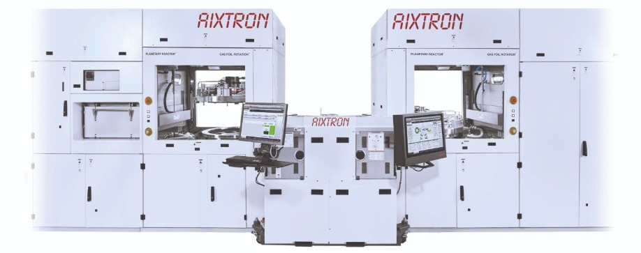
Figure 11. The latest (2020) G5+ C dual Planetary Reactor module cluster featuring cassette-to-cassette wafer handling.


