
Indispensable indium
From flat panel displays to semiconductor wafers, the use of indium in electronics continues to grow.
By Robert Ploessl, Indium Corporation
The element with atomic number 49 – indium – is central to modern life. Just consider a typical day: often we will spend hours staring at a flat panel display containing hundreds of thousands of pixels, each turned on and off by thin-film transistors and illuminated by some form of LED. While these transistors and LEDs might contain indium, there is no doubt that this element is encountered by the light traversing the display stack, as it will pass through indium-tin oxide (ITO) electrodes. This oxide combines transparency with conductivity, making it a great material for the display industry. In some of the latest high-colour-gamut TVs, indium crops up again, appearing in the display’s InP quantum dot layer of the colour filter that yields brilliant reds and greens. This makes five potential encounters between photons and indium-based materials before the light hits our retina. And there may be even more. If we watch content stored remotely, such as streaming video, it will reach us through a network of optical fibres, transmitting infrared light generated by an InP-based laser.
For those of us that are reading this on an electronic screen, the chances are that most of the above applies – there is no doubt that indium seems to be everywhere. Yet, despite its ubiquity, the economics of indium are poorly understood. That’s because most of the building blocks of modern technology emerge from supply chains that are rarely discussed, even in the technical press. To put it frankly, most of us don’t have much of a clue where indium comes from.
Let’s go back to the beginning. Like all heavy elements, indium was created during supernovas as planets condensed and formed. Due to its geo-chemical properties, indium appears in sphalerite, the most common ore of zinc, where its concentration can be as high as 100 parts per million. Another common carrier element for indium is lead. Deposits containing relatively high concentrations of indium are found all over the world. According to an exhaustive survey detailed by Ulrich Schwarz-Schampera and Peter Hertzig in Indium: Geology, Mineralogy, and Economics, a large number of indium-bearing deposits have been found around the Pacific Rim and in many other sites in Europe, Africa, and central Asia.
It comes as a shock to many, including quite a few working within the semiconductor industry that there are no indium mines anywhere. Element 49 is almost always co-mined with zinc. That’s not actually too surprising, as there are only a few carrier elements that have their own corresponding production infrastructure, such as copper, iron, and aluminium. When demand swings for most co-mined elements, such as indium, supply at the carrier infrastructure is often relatively inelastic. The real supply for indium is actually set downstream from the mines at the refiners where material is processed to produce an indium content up to 4N (99.99 percent). Indium ore is found all over the globe but refiners are heavily concentrated in China.
The overall global abundance of indium is in the range of 5-7 parts per million. That may not seem like a lot, but it is almost exactly the same value as that for silver. However, unlike that precious metal, which has been in use since ancient times, indium only started its commercial life in the twentieth century and was initially explored for its mechanical properties. One of the first successful applications of indium began in the 1940s when engineers diffused this metal into the surface layer of the bearings in aircraft engine pistons. Indium provided lubrication on the atomic scale, reducing wear and tear on the engine and increasing fuel efficiency – a prime example of our strongly held belief at Indium Corporation that materials science changes the world.
Fast forward to the age of electronics and high-speed communication when InP semiconductor crystals came to the fore, thanks to a bandgap that matches the transmission window of optical fibre. With a light source and a lossless technology for transmitting information, the groundwork was laid for the Internet and the connection of computers. It is a success story that we all know.
The InP-based lasers in optical networks are built on wafers sliced from monocrystalline boules, which are grown using techniques such as vertical freeze gradient and the Czochralski method – both requiring high-purity indium ingots as the starting ingredient. It is not sufficient to use standard commercial indium metal, which has a purity that starts at a 4N. That purity is suitable for making inorganic compounds and ITO sputter targets, but is not nearly enough for the production of compound semiconductors, which require a purity at least 500 times higher, typically 6N5.
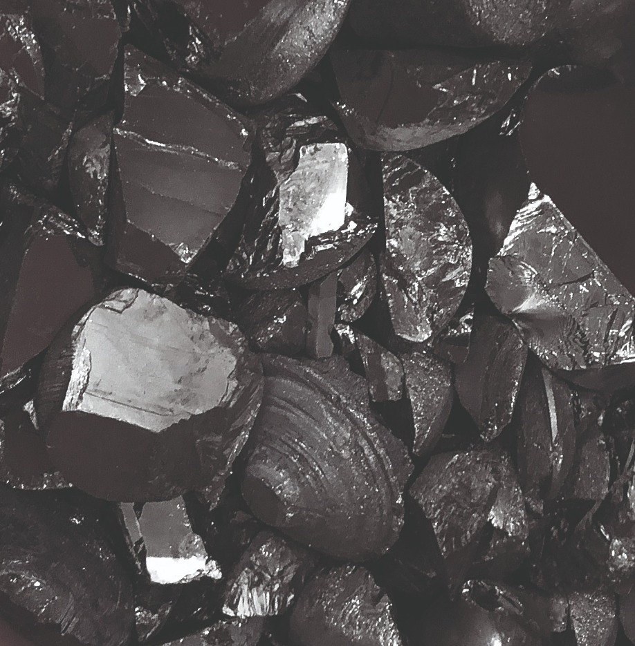
Indium phosphide crystal pieces from wafer boule manufacturing – the raw material for reclaiming indium from InP.
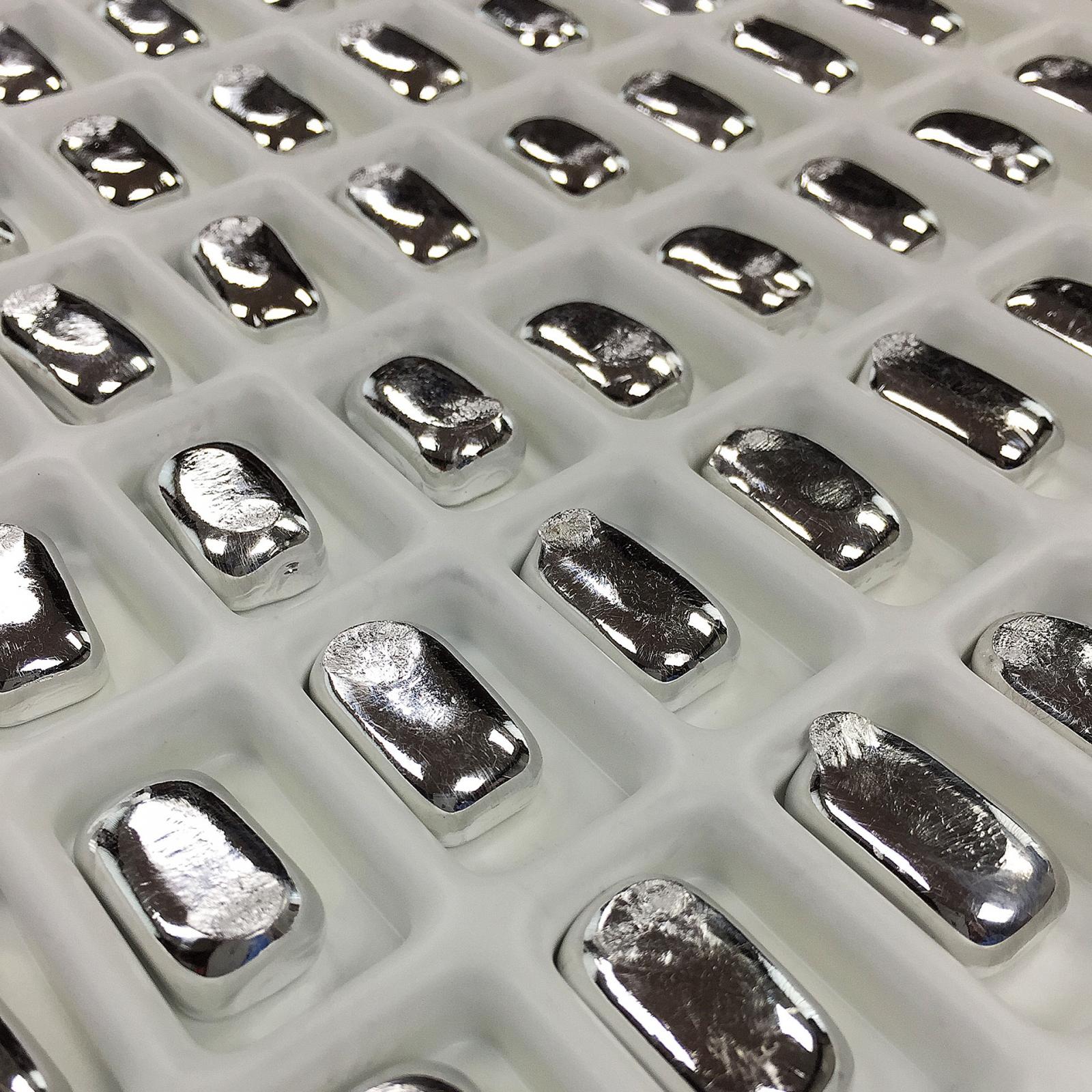
Indium with purity this high is produced in a cleanroom-like environment using a proprietary manufacturing process. The metal is cast into moulds with a wide variety of shapes and sizes. Ingots can be long cylinders, small 50-gram blocks or large rectangular shapes – anything that aids the downstream process for customers. It is critical to reduce trace elements, as they threaten to form energy states in the band gap of the InP semiconductor that degrade electronic and optical properties. Unwanted consequences of undesirable states include a lowering of electron mobility, a decrease in photoluminescence efficiency, and the creation of carrier recombination pathways.What happens to the InP crystals and wafers that are left over from their respective manufacturing process? What about the sustainability of the indium value chain?
From the start, the ITO and flat panel display industry have been reclaiming indium and the compound semiconductor industry is now following suit. This is to be expected, as every mature, high-value-added materials-using industry should have a recycling loop for its valuable input materials. At Indium Corporation we have added this reclaim capability, initially for InP crystals and wafers, and we plan to add capabilities for InSb in the near future.
There is no doubt that it makes sense to do this at the industrial level with end-of-life wafers and unused crystal material. It is harder to accomplish this with packaged electronic InP devices or end-of-life consumer products – this probably explains why we are not aware of any companies doing so. However, if our society is to be a responsible steward of our planet, this is an important objective.
As of today, we are concentrating on output from crystal growers, InP wafer makers, and output from fab and epi-wafer fabs. If you are using InP wafers in a fab and have any recycling needs, we certainly would like to hear from you.
So, what does the InP-consuming industry landscape currently look like and how has it evolved? 25 years ago, this magazine reported that global InP wafer consumption totalled 58,000 wafers, equating to a surface area of 183,000-square inches. Back then, Japan led the world and was responsible for 56 percent of wafer consumption. Today, according to a recent report from SEMI, 64 fabs are capable of processing InP wafers – 40 percent are found in North America, 31 percent in Europe, and the balance in Asia. This report claims that the capacity figure of all these InP fabs, based on 200 mm equivalent wafers, totals 667,000. That’s a figure that equates to just over 11 times that of global consumption in 1995. So, it is clear that there has been an astonishing growth of InP, even with the caveat that the SEMI figures are capacities, rather than actual output. They are total fab capacities; that is, the InP output is in the mix but not the total number.
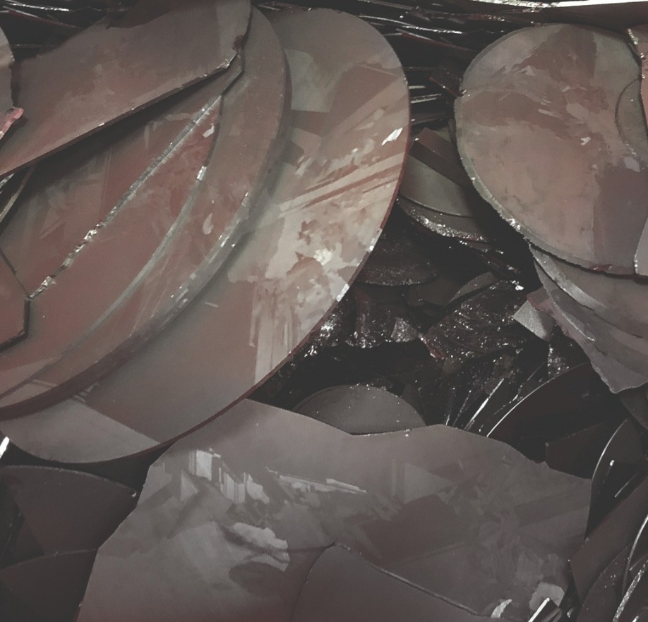
Polycrystalline InP wafers form part of the input stream for indium reclaim.
Up until now, we haven’t discussed other semiconductor wafers that incorporate indium – InSb and InAs. Due to their narrow bandgaps, these wafers are used primarily for the manufacture of infrared sensors and detectors. Reliable market figures are sparse. However, this could change very soon with the adoption of gas sensors and infrared imaging devices in, for example, the automotive sector.Another use of indium is, of course, in indium-containing epilayers. They are grown epitaxially, often by MOCVD, using the metal-organic trimethyl-indium. This source is made from high-purity indium trichloride, available as an anhydrous salt. The density of this salt may be tailored to the process of our customers.
When engineers use trimethyl-indium to grow heterostructures by MOCVD, they control the flow of this source of indium. With this lever, they tune the band structure and shift the emission or absorption wavelength of a device. An exciting new development over the last few years is the development of hybrid integration, a technology that allows compound semiconductor layers to be constructed directly on a silicon substrate.
As this technology is still in its infancy, outside the display market the growth of indium consumption is largely driven by data centres. They are the workhorses for the cloud, which has become both the storage and the processor of internet core computing. The cloud holds messages, photos, videos; it hosts entire web sites; and it runs software algorithms like machine learning. And if you are reading this online, the article will be stored there and brought to you via InP lasers to a screen coated in ITO, probably backlit with InGaN-based LEDs.
U. Schwarz-Schampera, P. M. Herzig, Indium – Geology, Mineralogy, and Economics, Springer 2002
SEMI report: SEMI – Power & Compound Fab report 2013 to 2024Jan 2013 to Dec 2024, update April 24, 2020 Edition https://www.semi.org/en/news-resources/market-data


