
Making microLED displays with a fluidic assembly process
Fluidic assembly of GaN microLEDs yields low-cost displays with better performance, efficiency and lifetime than those made with LCDs and OLEDs
BY PAUL SCHUELE, KURT ULMER, KENJI SASAKI AND JONG-JAN LEE FROM ELUX
MicroLED displays are made by integrating two mature, multi-billion dollar technologies. One is the GaN LED, developed for general lighting; and the other is the large-area, active-matrix backplane, developed for LCD and OLED displays.
The manufacture of a microLED display involves making LEDs with diameters of just 5 µm to 100 µm and using them to form the subpixels that provide direct emission. Compared with LCD displays, this mode of operation provides a far higher efficiency, alongside a very high contrast – it is over 50,000:1. The technology also outperforms OLED displays, which suffer burn-in effects and cannot realise as high a brightness.
Market penetration of microLED displays is tipped to begin with: large information displays that require high brightness; home theatre applications, which will benefit from increased dynamic range; and automotive displays, as they place a premium on high contrast and reliability.
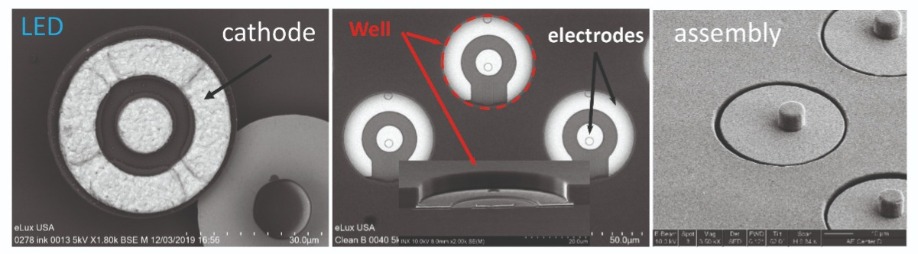
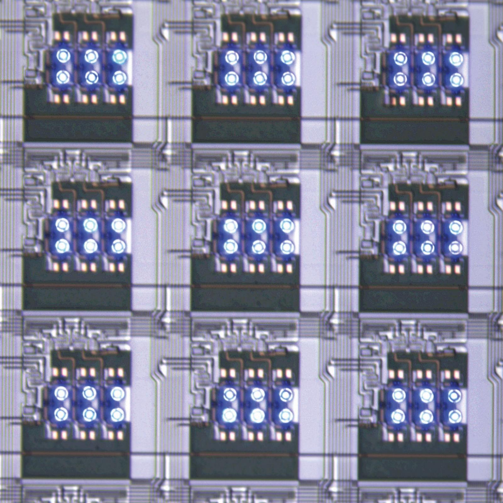
Figure 1. Scanning electron microscope images of: 40 µm microLEDs (left), matching electrode and well structures on a display substrate (centre), and assembled cells (right). The central image shows matching electrodes on the display backplane, and the cylindrical trap structure used to capture a microLED.
Developers of microLED displays are not finding it easy to fulfil the promise of this technology because they face a unique manufacturing challenge: how to position and connect millions of small devices at low cost, while ensuring zero defects. High Definition displays have 1920 x 1080 pixels, and in UHD (4K displays) and 8K displays there are 3840 x 2160 pixels and 7680 x 4320 pixels, respectively. This implies that the manufacture of an 8K display requires the perfect assembly of 99.5 million microLEDs. While conventional pick-and-place tools are up to the task of positioning microLEDs with the required micron-scale accuracy, the throughput of serial assembly is inadequate. This weakness can be addressed with mass-transfer methods, but they struggle with pixel pitch and the exclusion of defective microLEDs.A very promising alternative, tackling all these challenges, is a massively parallel fluidic assembly process developed by our team at eLux of Vancouver, WA. The technology we are pioneering positions each microLED by capturing it in a trapping structure, which contains the electrodes connected to the display control circuitry.
Typically, our process begins with microLEDs emitting at 450 nm, that are 40 µm in diameter and have a thickness of about 4 µm (see Figure 1 for typical scanning electron microscope images of these flat disc-shaped structures). These microLEDs, fabricated from conventional GaN-based blue LED wafers, are flip chips featuring anode and cathode electrodes on the same surface, arranged as concentric rings. By using a low-temperature solder for the electrodes on the microLED, we connect them to substrate electrodes by an annealing process that takes place after fluidic assembly (see right image in Figure 1, showing the display after assembly, with microLEDs populating each of the assembly sites).
The binning challenge
The microLEDs we deploy in our microLED displays are fabricated from wafers that are like those used for general lighting. The advantage of this approach is that the cost-per-device is very low – but it also introduces problems unique to microLED technology.
Figure 2. During microLED fluidic assembly, post-down orientations are unstable, due to the parabolic fluid velocity profile at the display panel surface.
When deployed in lighting, the LED’s key characteristic is the cost-per-generated-photon. This must be low to minimise the cost of the light bulb. That constraint has led the makers of LEDs to include a binning process, to account for process variability and defects. Briefly stated, after each LED is packaged, it is tested and ‘binned’ into a comparable group, based on efficiency and emission wavelength characteristics. If devices are defective, they are discarded. By adopting this approach, MOCVD fabrication is cheaper, because it minimises the costs associated with defect reduction and process control methods.For microLEDs, this modus operandi is an issue. Even in the most expensive, state-of-the-art microLED fabs, defectivity levels are still 0.1 percent or more. The imperfections result in dark sub-pixels, which are unacceptable in display products.
Unfortunately, it is impractical to identify and discard defective microLEDs using a binning process. Handling and functional testing these tiny devices is difficult, due to their diminutive size, their lack of packaging and the incorporation of electrodes. With a UHD display requiring at least 24.8 million microLEDs, testing times are too long to be practical. What is needed are new structures and methods that prevent defective microLEDs from ruining displays with defective subpixels.
To meet this challenge, our production process begins by mapping the defects on the microLED wafer. A variety of methods can accomplish this, including optical inspection, micro-photoluminescence, electroluminescence and cathodoluminescence. Armed with this mapping data, it is a simple matter to selectively harvest the good microLEDs. They form part of an ink used in our fluidic assembly process, while defective devices are discarded. Making displays from only known good microLEDs is one of the unique advantages of the fluidic assembly method.
Fluidic assembly
Our fluidic assembly process allows us to pass a liquid suspension of millions of microLEDs over a substrate that is populated with an array of trap sites, arranged as display pixels. As the microLEDs are similar in size to red blood cells, many of the suspension handling methods are like those used to handle biological samples. Once the microLEDs have settled, the suspension is forced to flow across the substrate, pushing devices across the surface and over the trap sites. Many assembly attempts occur randomly every second, thanks to numerous microLEDs and trap sites. Thus, stochastic assembly is massively parallel, and proceeds very quickly compared with competing deterministic assembly processes, where speed is limited by the mechanical characteristics of a pick-and-place head, or the mass transfer stamp.
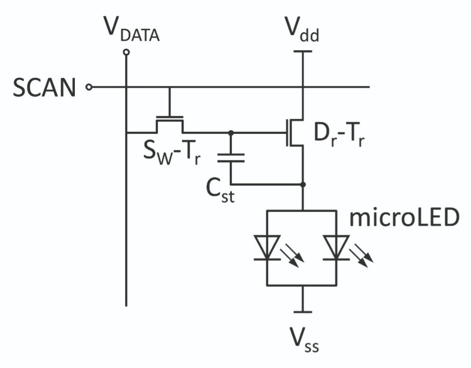
Figure 3. A two-transistor TFT circuit for a display sub-pixel.
Note that scaling up our fluidic assembly method to very large glass, such as Gen 6 (1500×1850 mm), is relatively simple. All that is required is a large tray to hold the ink, and a longer liquid-forcing apparatus. In comparison, it is far more taxing to develop mechanical assembly tools for very large areas.To ensure that fluidic assembly is a success, most assembly attempts should employ the correct orientation of the LED, and make sure that once a device is trapped, it must never escape. The likelihood of these occurrences is increased by engineering the shapes of the trap structures and the microLEDs, which feature a protruding post. This ensures that during fluid flow desired orientations and positions are stable, while undesirable configurations are unstable.
One important consideration is the fluid velocity. As this decreases parabolically to zero at the display surface, the microLEDs that are pushed along by the flowing fluid are subjected to a varying force that increases with height. Consequently, microLEDs that have their protruding post facing downwards tend to flip over to a post-up orientation, which has lower applied force (see Figure 2, upper left). This means that after a short time, all microLEDs on the surface are in a post-up orientation.
A second line of defence is that even if a post-down device is captured by a well (see Figure 2, lower left), there is a significant cross-sectional area exposed to fluid flow. This will cause the mis-oriented microLED to flip out of the well, settle to the surface post-up, and then assemble in another open well somewhere down stream.
It is critical that the trap sites are a good fit for the shape of the microLEDs, as this ensures that most assembly attempts result in a microLED falling into a trap and stopping (see Figure 2, lower right). We accomplish this with cylindrical wells that are slightly larger than the diameter of the microLED discs and deeper than their thickness. Depth is essential, minimising the de-trapping force on an assembled microLED and allowing other microLEDs to flow over it.
Making displays
We make our microLED displays on a glass substrate, using an array of thin-film transistors (TFTs) to control the current to each LED. The sub-pixel circuit has an access gate and a current-control transistor that drives two microLEDs in parallel, with the current set by the charge stored on the storage capacitor (see Figure 3). By using two-fold redundancy, we can compensate for one unconnected microLED – in that case, all current passes through one device, producing a similar amount of light to two devices in parallel.
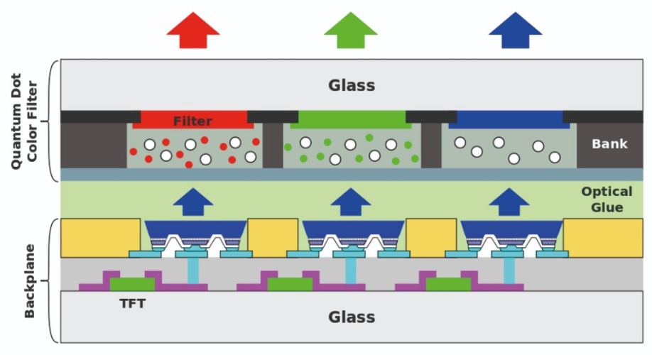
Figure 4. Red, green and blue pixels are formed by combining blue-emitting devices with quantum-dot phosphors.
To produce an RGB pixel, we use an optically transparent glue to laminate the display backplane containing TFT control circuits and the assembled blue microLEDs to a quantum-dot colour filter sheet (see Figure 4). Two features of the quantum-dot colour filter glass are: a structure set by the black matrix and bank material that prevents photons from travelling between adjacent pixels; and a form that defines the printed quantum-dot layer. The quantum dots are key to the operation of red and green pixels, which produce their colour by absorbing blue emission and re-emitting at longer wavelengths. For blue sub-pixels, the printed material scatters the blue light from the microLEDs, to replicate the isotropic distribution of light emitted from the quantum dots.
The conversion efficiency of the red and green quantum dots is about 60 percent, so to meet the desired colour temperature, the white point of the display is adjusted to 6500 K by decreasing the intensity of the blue sub-pixels (see Figure 5). The display has a colour gamut area 116 percent of NTSC and the white point matches D65 (see Figure 6). By further tuning the quantum dot colour filter, we can extend the colour gamut. A pixel-by-pixel mura correction can adjust the intensity and colour balance of each pixel.
Multiple market opportunities
MicroLED displays offer several advantages over current display technologies, including a far higher brightness, high contrast, a wide colour gamut and high reliability. However, development is still at an early stage. For an overview see Table 1, which outlines the prospects for microLED displays in several different product categories, and also offers a rough estimate of the degree of difficulty and the amount of development still to be realised to make each one a success.
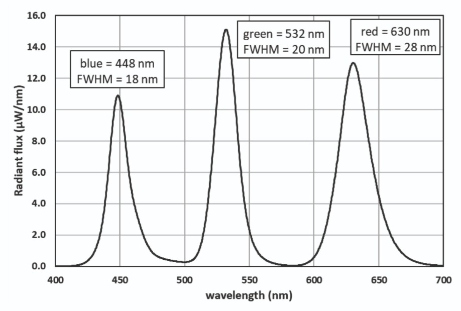
Figure 5. The white point spectrum of the eLux microLED display with a colour temperature of 6500K (D65).
An early implementation of microLEDs is in the very large public information display. The requirements for high brightness, no burn-in and large pixel size are ideally met, but prices today are astronomical, with costs exceeding $20k/m2. We believe our technology can be a game-changer, thanks to the very low-cost of fluidic assembly.
Virtual reality and augmented reality are very attractive markets for small size displays. Success is challenging, however, as to meet the requirement for very high resolution, microLEDs must be very small. When shrinking dimensions to below 10 µm LED efficiency plummets and the pixel sizes are too small for quantum dot colour conversion. Compounding the situation, it is unclear how to assemble three colour emitters to make an RGD display. Consequently yield, cost and heat dissipation are serious issues for VR/AR applications of microLEDs. Because it may not be possible to use fluidic assembly when microLEDs dimensions are below 5 µm, we are not planning to address VR/AR markets.
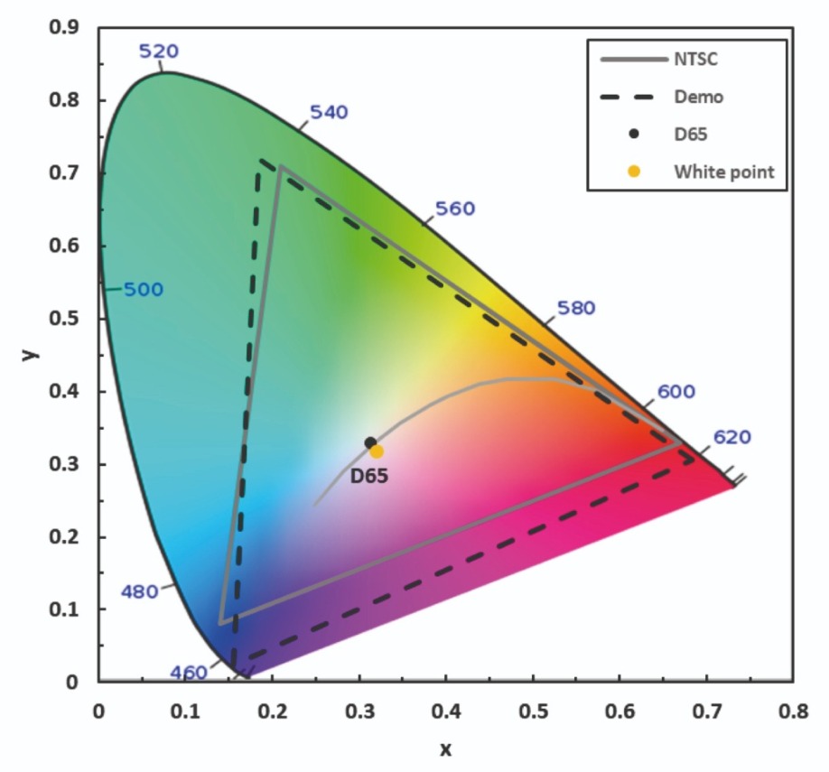
Figure 6. Colour gamut of the eLux microLED display showing 116 percent of the NTSC gamut and a white point set to D65.
One long-term goal of eLux is the adoption of our technology in television. This is the largest market opportunity for this technology, with microLEDs providing higher brightness, no burn-in and comparable contrast compared with the leading high-end technology, OLEDs. Success here is harder than in public information displays, which can tolerate a few defective pixels, because the television market demands 100 percent yield, flawless images and competitive pricing. In our view, if microLED televisions are going to have an impact, they will need to be perfect, while retailing for no more than $2,000. Stepping-stones towards that tough target are large home theatre installations, followed by professional displays.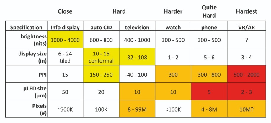
Table 1. Properties of microLED displays for different products. Cell colour represents level of difficulty to realise the required performance. Clear cells are achievable now, yellow will be difficult, orange extremely difficult and red is hard to imagine.
With our fluidic assembly technology, we are able to use simple, low-cost equipment to realise assembly rates up to 50 million microLEDs per hour. That is by no means the limit – we anticipate production equipment could assemble an 8K display with 100 million LEDs in just a few minutes. As our technology is suitable for microLEDs with diameters ranging from 5 µm to 100 µm, it could be used to produce a wide variety of displays with resolutions from 800 ppi to 10 ppi. It is also possible to change the microLED emitter area independently of the assembly technique, allowing an increase in brightness to more than 5,000 cd/m2.Another opportunity is to switch from using colour-converters to direct-emitting LEDs, with blue and green GaN emitters joined with red-emitting, AlGaInP microLEDs that are assembled in the same way. We are looking forward to the future, given the great promise that the combination of microLEDs and fluidic assembly technology has for revolutionising the low-cost manufacture of displays for a wide range of products.
Further Reading
M. Boncheva et al. MRS Bulletin 30 736 (2005)
K. Ding et al. Appl. Sci. 9 1206 (2019)
T. Wu et al. Appl. Sci. 8 1557 (2018)


