
Building better solar cells

Better-performing solar cells result from the introduction of dilute nitrides, novel separation layers and germanium-on-silicon templates
BY RICHARD STEVENSON
What do we look for from a solar cell? Many seek a high efficiency, especially if they need to generate a lot of power from a small plot. Cost is also crucial, as the return-on-investment is a big factor in determining whether a power-generation project gets the go-ahead. And depending on the application, flexibility of the cells may be essential; as can the ability to deliver plenty of power after continual bombardment from high levels of radiation.
Excelling on some of these fronts while struggling on cost are multi-junction cells involving III-Vs. By combining record-breaking efficiencies with a relatively high radiation hardness, they can reign supreme in the space market, where cost is not a major consideration. For the emerging market of powering light-weight unnamed aircraft they also show much promise, because they can cover a curved surface and produce a lot of power. But they have failed to make an impact in generating electricity for the grid because they are too pricey, even when deployed in concentrating photovoltaic systems.
If the cost of making multi-junction cells were to fall, this would increase margins, and could lead to a growth in sales across the board. Success in this regard might result in a significant reduction in the cost-per-Watt, which could also fall through increases in efficiency – an improvement that is welcome in all applications. It is also a good idea to devote some effort to refining the fabrication and performance of flexible cells, given that this is a potentially lucrative application where this class of device can shine.
Efforts to increase efficiency, cut costs and develop processes for making flexible cells were discussed at the 37th European PV Solar Conference and Exhibition (EU PVSEC), held online between 7th and 11th of September 2020. Speaking in a session entitled III-V and Related Compound Semiconductor Solar Cell Devices, Ivan Garcia from The Technical University of Madrid outlined efforts to trim the cost of multi-junction solar cells by switching to growth on silicon substrates; Arto Aho from Tampere University, Finland, presented results related to the development of dilute nitride cells that could boost multi-junction cell efficiency; Nobuaki Kojima from the Toyota Technological Institute in Nagoya, Japan, detailed the use of a GaSe buffer for epitaxial lift-off of GaAs cells from a silicon substrate; and Christina Honsberg from Arizona State University spoke about the addition of GaPN top cells to form devices based on silicon that feature three terminals.
Cutting costs with silicon
Historically, germanium substrates have been used for manufacturing III-V cells, primarily because this foundation is cheaper and stronger than GaAs. Building on this approach, Garcia and co-workers from The Technical University of Madrid, working with engineers from the global epiwafer provider IQE, are pioneering germanium virtual substrates, created by the direct growth of germanium films on silicon. Merits of this approach include low cost, minimal germanium consumption, an absence of graded buffers, and the realisation of very low threading dislocation densities – values of just 5 x 105 cm-2 are possible.
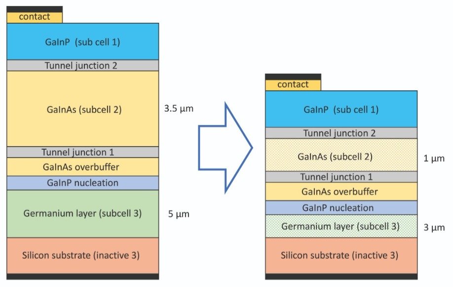
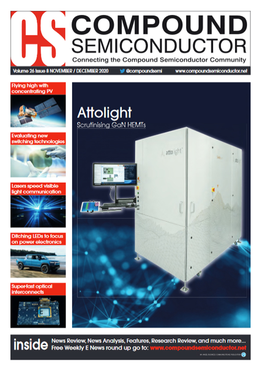
Figure 1. Reducing the thickness of the multi-junction cell that is grown on silicon leads to a reduction in the density of cracks in the epistructure.
However, success with this approach is not easy. When Garcia and co-workers started to use this foundation for the growth of multi-junction heterostructures, they found cracks in the epiwafers. This issue stemmed from the thickness of the epi-stack, with layers of germanium and the III-Vs totalling a thickness of around 10 μm. The critical thickness for the propagation of cracks is around half this value.Garcia’s explained that the team is addressing this issue by trimming the thickness of the epi-stack to 5.5 μm. This goes below the critical thickness, trading a far better material quality for a slight reduction in efficiency. The germanium layer that forms the bottom sub-cell is reduced from 5.5 μm to just 3 μm, and the middle sub-cell that is made from GaInAs is decreased from 3.5 μm to 1 μm (see Figure 1).
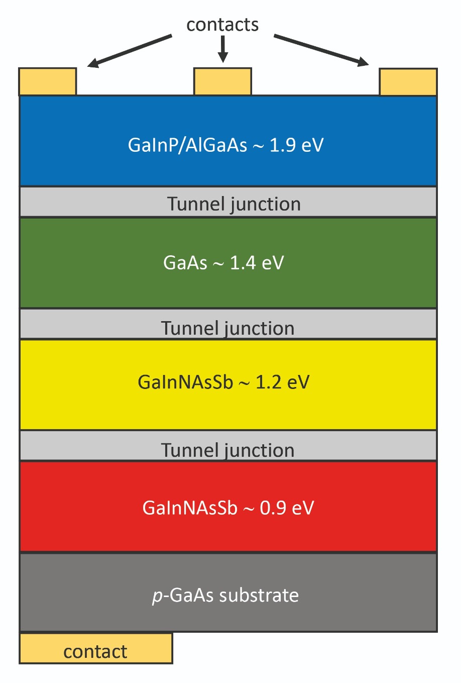
Figure 2. Researchers involved in the EU project AMETIST – Advanced III-V Materials and Processes Enabling Ultrahigh-efficiency Photovoltaics – are laying the foundations for devices with six or more sub-cells that involve dilute nitrides.
The team turned to modelling to assess the impact of the new design and investigate whether they needed a different composition to optimise performance. Based on considerations of the short-circuit current and the open-circuit voltage of the InGaAs sub-cell, they decided to employ an indium content of 8 percent in this 1 μm-thick layer.Another finding from this theoretical study is that the thinning of the cell reduces efficiency by 2-3 percent. Under concentration, the efficiency of this new design could still be as high as 39-40 percent.
By fabricating the two designs, the researchers found that thinning the epistructure reduced cracks from more than 5 per millimetre to less than 1 per millimetre.
The team also studied a device with just the bottom two cells. This revealed that thinning InGaAs increases carrier collection efficiency. However, the external quantum efficiency still lags that of devices made on germanium substrates.
For the team’s triple-junction cell, measurements under a 1 sun concentration showed that trimming the thickness led to an increase in current density, while the drop in open-circuit voltage is smaller than anticipated. However, performance is still significantly behind that of the standard III-V cells grown on silicon substrates, due to inferior material quality.
Goals for the future include investigating cells produced on higher-quality germanium-on-silicon templates and introducing current-matching in designs with thinned layers of GaInP and/or AlGaInP. Efforts may also be directed at evaluating residual tensile strain in thinned structures and considering the implications of this.
Delivering with dilute nitrides
One of the most effective ways to increase the efficiency of multi-junction photovoltaics is to replace the germanium sub-cell with multiple variants formed from dilute nitrides. This alternative design helped NREL to raise the record for efficiency to 47 percent, using a six-junction device; and it is also being pursued through a European project running from 2017 to 2022 entitled AMETIST: Advanced III-V Materials and Processes Enabling Ultrahigh-efficiency Photovoltaics. The latter aims to realise an efficiency of 55 percent with a monolithic cell featuring GaInNAsSb and GaNAsBi layers and nanophotonic structures for light-trapping.
Figure 3. A team from Arizona State University is developing a three-terminal solar cell that incorporates a lattice-matched dilute nitride.
Aho, who is working on this project, told those tuning in to EU PVSEC that the team’s devices have their pros and cons compared with those formed by wafer fusion and mechanical stacking. Approaches of this ilk, which have produced efficiencies as high as 46 percent, are complex and expensive, with two wafers needed to form a device; but designs are free from material compromises. For developers of monolithic devices, decisions have to be made between upright and inverted designs, and lattice-matched and metamorphic architectures. The lattice-matched upright design adopted in the AMETIST project is simple to process and allows the use of the same tunnel junction throughout, but epitaxy is not easy to master.Simulations by the team highlight the promise of their dilute nitrides. Triple-junction cells should be capable of efficiencies of 49 percent, rising to values of 52 percent and 55 percent for variants with six and eight junctions.
Updating delegates of progress made during the first few years of the project, Aho presented results of efforts at producing four-junction cells with two dilute nitride sub-cells (see Figure 2). Measurements on cells with a size of 2 mm by 2 mm show an efficiency of 39.3 percent at 564 suns, falling to 36.9 percent at 946 suns.
Analysis revealed total losses of 15 percent. Of this, 6 percent came from grid and shadowing losses, with the team believing there is only room for marginal improvements; just 1 percent was associated with transmission losses from the upper tunnel junction; and 8 percent came from transmission and/or collection losses in the bottom cell – this is where there is an opportunity for the biggest gains.
The team have started to develop sub-cells that could be added to the device to increase efficiency. Work has been directed at a sub-cell with a bandgap of more than 1.9 eV, and another below 0.9 eV. During the project the team developed techniques to increase the nitrogen content in GaInNAsSb layers, and fabricated AlGaInP devices with a bandgap of up to 2.18 eV that have an efficiency up to 26 percent. “We have the building blocks for six-junction solar cells,” remarked Aho.
Flexible photovoltaics
Production of flexible thin-film photovoltaics has much to offer, combining the opportunity to cover curved surfaces with the potential for substrate re-use. This technology has been developed by inserting an AlAs buffer between a GaAs substrate and a cell made with the same material, with HF etching removing the sacrificial layer. However, etching is time consuming and substrates are expensive.
Addressing these weaknesses, Kojima and co-workers are trailblazing the use of a two-dimensional metal selenide layer that allows mechanical cleavage and re-use of the silicon substrate. To ensure success, the two-dimensional structure has to be thermally stable under the growth conditions used for GaAs.
Promising materials for the two-dimensional metal selenide layer are In2Se3 and GaSe, materials with lattice constants relatively close to that of GaAs. Using diffraction patterns generated during MBE of III-Vs on silicon, the team observed how the growth of In2Se3, followed by GaAs, created a layer of Ga2Se3. Although the direct growth of Ga2Se3 on silicon is possible, it yields films with inferior material quality.
To separate the GaAs-based epilayers from the silicon substrate, Kojima and colleagues bonded the top of the wafer to a polymer sheet with an adhesive, before dipping the resulting structure in liquid nitrogen. A homogeneous thermal stress resulted, separating the substrate from the GaAs layers.
Inspecting the silicon substrate with a scanning electron microscope uncovered flaky remains on its surface, while optical microscopy revealed plenty of wrinkles in the GaAs film produced by the peeling process. This suggests more progress is needed before this technology can realise its full potential.
Supplementing silicon
While III-Vs can’t compete with silicon on price, they will always hold the ascendancy on efficiency. The best value for silicon is now just shy of 27 percent, with any gains modest and hard to come by. But what about adding a III-V to silicon to try and enjoy the best of both worlds? That’s the approach adopted by Honsberg and her team from Arizona State University.
She told the on-line attendees at EU PVSEC that a major impediment to this approach is the lack of a conventional III-V that is latticed matched to silicon and has a suitable bandgap – ideally, it needs to be around 1.7 eV. Her solution is a three-terminal solar cell that incorporates a lattice-matched dilute nitride (see Figure 3). By turning to a three-junction solar cell, the current-matching constraint is alleviated while allowing monolithic integration. Honsberg explained that the three-terminal tandem is relatively unsensitive to optimisation of the bandgap, allowing the use of higher bandgaps that result in a greater proportion of energy from the silicon cell. She also pointed out that to get the best output from the tandem, the bandgap of the top cell needs to be higher when working with imperfect material.
To prevent damage from the nitrogen plasma, as well as deleterious effects of nitrogen at the silicon interface, Honsberg and co-workers employ a GaP buffer layer. Growing this on silicon can lead to anti-phase domains, misfit dislocations, stacking faults and pit formation, with the team from Arizona finding that they get their best results when using off-cut substrates. Working with an off-cut of 4° increased crystal quality, according to X-ray diffraction measurements, and improved minority carrier lifetimes.
Measurements on unoptimised layers of GaPN grown on silicon show a minority carrier lifetime of 28 ns at 78K. Based on external quantum efficiency fitting of an experimental device, the minority carrier lifetime at room-temperature is estimated to be 0.5 ns – it needs to be 1-2 ns for an efficiency of more than 35 percent. This is an encouraging result, as is an external quantum efficiency of an initial device of 25 percent. Efforts will now be directed at defect annealing for different growth conditions as this could lead to better material quality, and ultimately more efficient devices.
Progress made by Honsberg and her team – as well as the recent research at The Technical University of Madrid, Tampere University and the Toyota Technological Institute – highlight the value that III-Vs can bring to solar technology. It’s hard to see III-V cells replicating their success in space on earth any time soon, but progress in the lab could spark commercial ventures and the emergence of sales.


